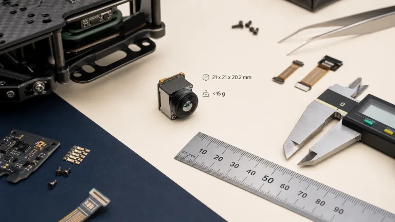
Thermal IR Camera Selection Guide for OEM & Embedded Systems Integration
Thermal IR Camera Selection & OEM Embedded Systems Integration Engineering Guide
Optical engineers, embedded systems architects, and industrial hardware designers face a tough technical fork when bringing infrared machine vision to life: balancing size, weight, power, and cost (SWaP-C) against spatial resolution, thermal sensitivity, optical transmission, and interface latency. Integrating an OEM thermal IR camera into an edge platform means cutting through consumer-grade marketing fluff and getting straight into uncooled focal plane arrays (FPAs), specialized optical physics, read-out integrated circuits (ROIC), and raw hardware transport layers.
Whether you’re developing a low-power smart home sensor, an autonomous aerial gimbal payload that has to clear strict aviation regs, or a rugged factory condition-monitoring node built to tight radiometric standards, your thermal core dictates processing overhead, thermal noise floor, and optical detection range. Here’s the deal: cutting corners on core architecture or bus bandwidth early in your schematic capture will burn months of bench re-spins later.
Table of Contents
- 👉 1. LWIR (8–14 µm) Thermal IR Camera Physics vs. Active NIR
- 👉 2. Uncooled Microbolometer Architectures: VOx vs. a-Si & NETD Dynamics
- 👉 3. Optical Engineering: IFOV, Germanium Optics, and Johnson’s DRI Criteria
- 👉 4. Embedded Host Interfaces: SPI vs. USB UVC vs. MIPI CSI-2
- 👉 5. Non-Uniformity Correction (NUC), Radiometric Calibration, and Thermal Drift
- 👉 6. OEM Product Showcase & Technical Evaluation: SuperMini 640 / 640T vs. AeroMini 640
- 👉 7. Edge AI Pipeline: Radiometric Processing with Embedded Frameworks
- 👉 8. OEM Engineering RFQ & Host Board Integration Checklist
- 👉 9. Frequently Asked Questions (OEM Engineering FAQ)
1. LWIR (8–14 µm) Thermal IR Camera Physics vs. Active NIR
To integrate infrared optical hardware cleanly, your engineering team must distinguish Near-Infrared (NIR), Short-Wave Infrared (SWIR), and Long-Wave Infrared (LWIR). Band boundaries vary by convention: NIR is commonly about 0.75–1.4 µm and SWIR about 1.4–3 µm, while the cores discussed here respond over 8–14 µm. Standard silicon CMOS sensors used for 850 nm or 940 nm night vision lose sensitivity near 1.1 µm; they do not cover the entire NIR or SWIR range. Active illumination and passive thermal emission are different operating principles, rather than properties defined solely by a band name. Hamamatsu’s silicon detector specifications illustrate the silicon response limit.
Active NIR night-vision setups collect reflected illumination. A standard CMOS silicon sensor stripped of its IR-cut filter can collect 850 nm or 940 nm photons from auxiliary LEDs; ambient illumination can also contribute. Active lighting adds power demand. Fog, smoke, haze and dust can attenuate or scatter light, but performance depends on wavelength, particle distribution and path length. Compare the relevant conditions experimentally rather than treating either NIR or LWIR as a universal solution for obscurants.
Look at how a passive thermal IR camera operates instead: it senses thermal radiation within its LWIR response band, often 8–14 µm. Objects above absolute zero emit thermal radiation. The first expression below is Planck’s blackbody spectral radiant exitance, M(λ, T), per unit wavelength; the second gives total emitted radiant exitance E for a graybody with wavelength-independent emissivity ε:
E = ε σ T4
Where h represents Planck’s constant, c is the speed of light in vacuum, k is Boltzmann’s constant, ε is target emissivity, and σ is the Stefan-Boltzmann constant (5.670374 × 10⁻⁸ W·m⁻²·K⁻⁴). With λ in meters and T in kelvin, the Planck expression gives W·m⁻³; it is an exitance expression and therefore includes π. For -40°C to +500°C (233.15 K to 773.15 K), Wien’s Displacement Law (λmax × T ≈ 2897.8 µm·K) places the blackbody peak at approximately 12.43 to 3.75 µm. A detector samples only its response band, not the entire emitted spectrum; real surfaces can have wavelength-dependent emissivity. See NIST’s optical-radiation reference for the blackbody relationships.
An LWIR thermal IR camera can form images without visible illumination, but its received signal includes emitted and reflected radiation, with atmospheric attenuation along the path. Some smoke conditions favor LWIR; dense fog, rain, dust and opaque obstacles can still limit the view. Solar heating and reflected radiation can affect interpretation, and direct viewing of the sun can damage some cores. Quantitative temperature measurement requires a radiometric model and the appropriate calibration, emissivity and reflected-temperature corrections. If you’re building size-constrained inspection pods or robotics, our ir camera module drone OEM integration checks cover mechanical isolation, thermal paths and electrical noise filtering for the carrier PCB.
2. Uncooled Microbolometer Architectures: VOx vs. a-Si & NETD Dynamics
Modern uncooled thermal cores run on a Micro-Electro-Mechanical Systems (MEMS) focal plane array (FPA). Each active pixel is an ultra-thin suspended thermistor membrane held up by high thermal resistance micro-legs fabricated over a silicon Read-Out Integrated Circuit (ROIC). When incident LWIR radiation hits the membrane, the absorbed energy heats it up, shifting its electrical resistance. The ROIC reads the pixel responses and digitizes the signal. Converting those values to temperature requires a supported radiometric output mode and calibration; raw digital values are not automatically temperatures.
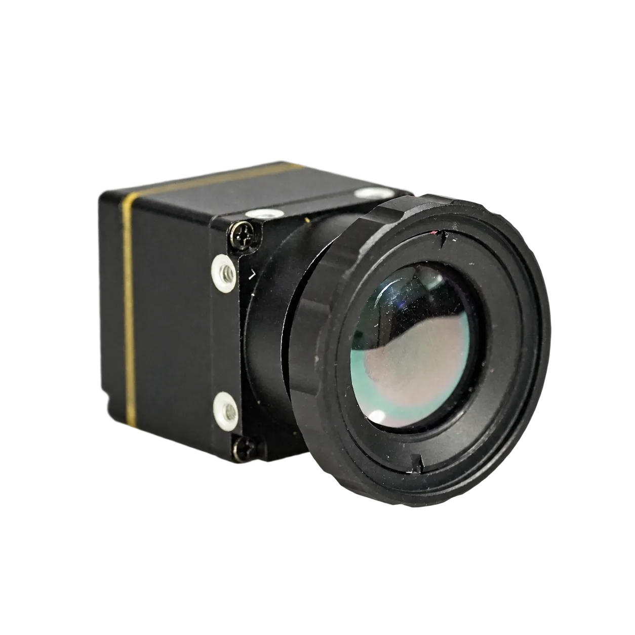
Figure 2: Illustrative angled view of a black camera housing with a circular lens and gold-colored seam. The image does not establish detector, interface or current-product specifications.
Vanadium Oxide (VOx) vs. Amorphous Silicon (a-Si)
The thin-film material deposited across that suspended bolometer bridge contributes to your sensor’s signal-to-noise ratio (SNR), thermal time constant, and operational stability:
- 🔬 Vanadium Oxide (VOx): VOx is widely used in uncooled thermal IR camera modules. Its resistance changes with temperature, allowing incident thermal radiation to be measured. TCR, noise and time response depend on the film process, pixel structure, readout and operating conditions; compare the finished detector or camera specifications rather than assigning a universal VOx performance tier.
- 🔬 Amorphous Silicon (a-Si): a-Si is another established microbolometer material with semiconductor-manufacturing compatibility. It is not inherently restricted to budget sensing or a fixed 50–70 mK NETD range. Material selection alone does not determine sensitivity, spatial detail, cost or system stability.
Noise Equivalent Temperature Difference (NETD)
NETD describes thermal sensitivity under specified measurement conditions. It is the small blackbody temperature change that produces a signal change equal to the measured RMS noise. A useful local measurement definition is:
Here σsignal is the measured RMS signal noise and dS/dT is the local signal response to blackbody temperature in the same signal units. State the target temperature, lens F-number and transmission, integration time or frame rate, filtering, and noise-measurement method when comparing NETD values. NETD is not absolute temperature accuracy or a guarantee that a small feature can be resolved. See LYNRED’s measurement definition.
A lower NETD can help distinguish subtle thermal contrast when spatial sampling, optics and the test conditions also support the task. The current AeroMini specification is ≤30 mK at 25°C, F/1.0, while SuperMini specifies ≤40 mK under the same stated temperature and F-number conditions. These numbers alone do not guarantee detection of subsurface defects, objects behind foliage or a particular fault size. A lower-resolution, low-power sensing design may still be appropriate for coarse HVAC trends or threshold monitoring; validate the whole system against the required contrast and feature size.
Pixel Pitch Scaling: 12 µm vs. 17 µm vs. 35 µm
Pixel pitch—the center-to-center spacing between neighboring bolometer pixels—affects active-array size and the choice of optics. Stepping down from older 35 µm or 17 µm pitches to 12 µm can reduce the footprint at a given pixel count. Smaller sensor dies use proportionally shorter focal length lenses to hold the same nominal Field of View (FOV). The resulting lens diameter, mass and cost still depend on aperture, material, element count and mechanics. Check optical MTF, diffraction, focus, sensitivity and processing together; a smaller pitch alone does not guarantee sharper imagery.
3. Optical Engineering: IFOV, Germanium Optics, and Johnson’s DRI Criteria
Standard visible-light optical glasses such as BK7 and fused silica generally provide inadequate transmission across 8–14 µm for LWIR imaging. Transmission depends on material, wavelength and thickness; “100% absorption” is not a useful universal specification. An LWIR thermal IR camera requires optical materials and coatings specified for its actual operating band.
LWIR Optical Materials Breakdown:
- 💎 Monocrystalline Germanium (Ge): Its refractive index is approximately 4 near 10 µm. Uncoated surfaces have substantial reflection losses, so suitable anti-reflection coatings are important. DLC can provide a durable outer coating, but transmission must be specified for the actual substrate, thickness, coatings and complete lens; neither a universal transmission value nor low chromatic aberration follows from the material name alone. See Edmund Optics’ material and coating specifications.
- 🧪 Chalcogenide Glass: Certain compositions support precision molding for repeatable production. Cost, transmission and temperature behavior depend on composition and the manufacturing process. Passive athermalization requires an optical and mechanical design that maintains focus across the specified temperature range; it is not an automatic property of every chalcogenide lens. SCHOTT’s infrared-glass data show composition-dependent optical and thermal properties.
Instantaneous Field of View (IFOV)
Instantaneous Field of View (IFOV) is the angular sampling interval of one detector pixel. For small angles near the optical axis, IFOV is approximately pixel pitch divided by focal length. It helps estimate scene sampling at a working distance; it is not by itself the minimum resolvable or temperature-measurable feature size:
For instance, mating a 12 µm detector with a 9.1 mm focal length lens produces an IFOV of 12 / 9.1 ≈ 1.32 mrad. At 100 meters, one pixel samples approximately 1.32 × 10⁻³ × 100 = 0.132 m = 13.2 cm in each direction near the image center. Optical blur, distortion and the number of pixels needed for the inspection task must also be considered.
Johnson’s Criteria: Operational DRI Modeling
Johnson’s Criteria are historical observer-performance models relating resolved spatial detail to detection, recognition and identification tasks under defined contrast, probability and viewing conditions. They are not a universal conversion from pixel count to field performance. Digital processing, optics, noise, scene contrast, atmosphere and the task definition all change the result:
- 🎯 Detection (D): Establishing that a feature of interest is present. State the scene, thermal contrast, false-alarm criterion and test procedure.
- 🎯 Recognition (R): Distinguishing the relevant feature class. Validate with representative inspection data rather than importing a universal pixel threshold.
- 🎯 Identification (I): Resolving the detail required by the task. Historical line-pair criteria are conditional observer results, not a product range specification or a design guarantee.
The following illustrative geometry uses a 640×512 detector with 12 µm pitch (7.68 × 6.144 mm active area), a rectilinear lens and negligible distortion. FOV is calculated as 2 × arctan(sensor dimension / (2f)); scene sampling uses the small-angle IFOV near the optical axis. These examples preserve the focal-length comparison for planning and do not describe current factory lens availability, guaranteed inspection resolution or detection ranges. See the focal-length and FOV geometry reference:
| Lens Focal Length | Calculated FOV (H × V) | Spatial IFOV | Sampling at 10 m | Sampling at 50 m | Sampling at 100 m |
|---|---|---|---|---|---|
| 4.9 mm | 76.2° × 64.2° | 2.449 mrad | 2.45 cm/pixel | 12.24 cm/pixel | 24.49 cm/pixel |
| 9.1 mm | 45.8° × 37.3° | 1.319 mrad | 1.32 cm/pixel | 6.59 cm/pixel | 13.19 cm/pixel |
| 13.0 mm | 32.9° × 26.6° | 0.923 mrad | 0.92 cm/pixel | 4.62 cm/pixel | 9.23 cm/pixel |
| 19.0 mm | 22.9° × 18.4° | 0.632 mrad | 0.63 cm/pixel | 3.16 cm/pixel | 6.32 cm/pixel |
| 35.0 mm | 12.5° × 10.0° | 0.343 mrad | 0.34 cm/pixel | 1.71 cm/pixel | 3.43 cm/pixel |
For further selection context, see our high-resolution thermal imaging camera OEM selection guide. Use the thermal imaging calculator for preliminary geometry with supported inputs, then confirm the ordered lens and measure performance on representative inspection scenes. Calculator outputs are not radiometric, AI or operating-range guarantees.
4. Embedded Host Interfaces: SPI vs. USB UVC vs. MIPI CSI-2
Picking the right electrical transport layer determines your MCU/SoC pin count, bus bandwidth, driver stack complexity, and system latency. Depending on model and firmware, an OEM thermal core may output display video, raw digital counts, calibrated temperature data, or a combination. Bit depth and connector type do not establish the meaning of the values or simultaneous-output support.
| Interface Protocol | Host Processor Class | Bandwidth & Payload | Power-Budget Check | Primary Application Fit |
|---|---|---|---|---|
| SPI (module-specific connector) | MCUs with a suitable SPI/DMA peripheral | Clock, packet format and usable throughput are module-specific | Measure the selected sensor, rails and host duty cycle | Lower-resolution sensing, smart appliances, HVAC monitoring |
| USB UVC; other functions if implemented | Linux/Windows IPCs and supported SBCs | USB 2.0 High Speed has a 480 Mbps signaling rate; usable video throughput is lower | Include the interface board and host USB load | Rapid prototyping and inspection imaging |
| MIPI CSI-2 (matched lane configuration) | SoCs with a compatible receiver and driver | Confirm lane rate, data type, timing and receiver limits | Include the core, receiver and processing workload | Embedded inspection and edge-AI image acquisition |
1. Serial Peripheral Interface (SPI) via Flexible Printed Circuit (FPC)
For compact, battery-operated designs, an SPI host bus can connect a suitable lower-resolution sensor to an MCU without a full operating system. Connector pitch, pin count, voltage, master/slave role, packet format and available frame rate are specific to the module. DMA can reduce CPU transfer work, but SPI itself does not specify sensor power, supply voltage or calibrated temperature output. Keep the low-resolution/low-power sensing trade-off separate from the 640×512 current-product comparison below.
2. USB Video Class (UVC) and Model-Specific Control/Data Paths
UVC can use an operating system’s standard video-class driver when the device implements a supported UVC format and mode. That does not guarantee every host or application can access all resolutions, frame rates, controls or radiometric data. CDC serial, HID and vendor-specific interfaces are distinct mechanisms; HID is not a virtual COM port. Verify the delivered USB descriptors, SDK and firmware rather than assuming parallel temperature output or a particular control endpoint. The USB-IF class definitions distinguish video, communications and HID functions.
3. MIPI CSI-2 (Camera Serial Interface 2)
MIPI CSI-2 can connect a compatible core or interface board to an embedded SoC camera receiver. Match the lane count and rate, voltage requirements, CSI-2 data type, frame layout, clocks and driver support. A RAW8/RAW14/RAW16 packet label describes transport packing, not automatic temperature calibration. MIPI does not guarantee zero-copy capture or a latency below 20 ms; measure exposure-to-host and end-to-end latency with the selected firmware and processing stack. See the MIPI CSI-2 specification overview for transport scope.
Current-Product Connector and Cable References
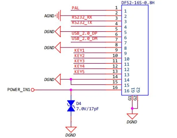
The AeroMini USB + CVBS + MIPI tailboard and Type-C + CVBS tailboard are separate configurations. The following 16-pin diagram belongs to the illustrated USB/CVBS board, not the Type-C board. The schematic labels RS232_RX/RS232_TX; confirm the supplied board’s electrical levels and any required transceiver before connection to TTL-level UART. POWER_IN1 on this 16-pin connector and POWER_IN2 in the separate 26-pin guide are 5 V inputs; do not apply 12 V. Confirm the supplied board revision, physical connector orientation and complete signal table before wiring.
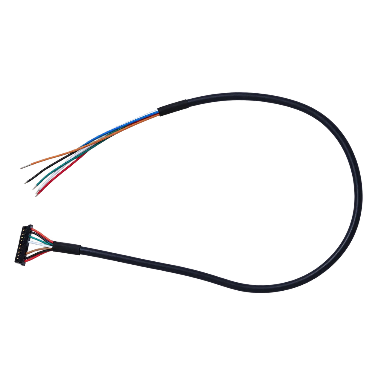
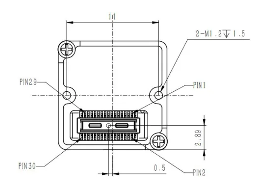
SuperMini uses a separate Hirose DF40C-30DP-0.4V(51) core connector, MAIN_POWER at 3.8–5.2 V plus +3.3 V and +1.8 V rails, and the manual’s power-on sequence. Its UART is 1.8 V logic with TX/RX referenced to the core, and CVBS requires an external video-buffer IC. Confirm output selection: BT656 and MIPI cannot operate simultaneously. The core connector drawing does not describe the optional USB expansion board.
5. Non-Uniformity Correction (NUC), Radiometric Calibration, and Thermal Drift
Microbolometer FPAs suffer from inherent pixel-to-pixel responsivity mismatch and offset drift caused by wafer manufacturing variances, ambient swings, and circuit self-heating. Without appropriate correction, fixed-pattern noise (FPN) and temperature-dependent offsets can degrade imagery; the rate and severity depend on the core and environment.

Figure 6: Illustrative compact black lens housing with an amber flexible circuit. Appearance reference only; no current model or pinout is identified.
Two-Point Non-Uniformity Correction (NUC) Architecture
During factory non-uniformity calibration, the thermal core can be exposed to uniform blackbody sources at two or more temperature points (for example, T1 = 15°C and T2 = 45°C; actual factory points vary). Per-pixel gain G(i,j) and offset O(i,j) terms are stored in the module’s calibration data. The FLIR NUC explanation illustrates the distinction between factory characterization and temperature-dependent correction, rather than specifying either CAMCUDA core. With the following offset sign convention, a simple linear correction is:
To battle thermal drift out in the field, OEM modules leverage two primary methods:
- ⚙️ Mechanical Shutter Flat-Field Correction (FFC): A shutter provides a relatively uniform reference used to update pixel offsets and reduce residual spatial non-uniformity. Whether the stream freezes and how long correction takes depend on the module and mode. Establish the trigger policy, invalid-frame behavior and settling time on the selected firmware.
- ⚙️ Shutterless Algorithmic NUC: Some modules compensate without a periodic shutter interruption, using measured internal temperatures, calibrated models and/or scene-based methods. Capabilities and artifacts depend on implementation and scene behavior. Neither shutterless operation nor FFC alone establishes absolute temperature accuracy.
Industrial Radiometric Measurement Compliance
For predictive maintenance equipment and electrical inspections, specify the required temperature uncertainty and validate it across the agreed target and ambient ranges, optics, warm-up and measurement setup. A blanket ±2°C or ±2% claim does not apply to every thermal core. The ASTM E1934-99a(2024) guide for examining electrical and mechanical equipment with infrared thermography addresses inspection practice; it is not a camera accuracy certification. Account for emissivity, reflected apparent temperature, atmosphere, focus and spot size. The imaging-only models below do not measure temperature.
6. OEM Product Showcase & Technical Evaluation: SuperMini 640 / 640T vs. AeroMini 640
To help you pick the right core for your schematic layout, here is a side-by-side engineering evaluation of two current 640×512 product families: SuperMini for bare-core, low-mass integration and AeroMini for a selected lens-and-tailboard assembly. Both require configuration review. For simpler coarse sensing, retain a separate lower-resolution/low-power sensor evaluation; neither featured family should inherit specifications from an older 160×120 SPI module.
Product Showcase 1: CAMCUDA SuperMini 640 / 640T Bare Core
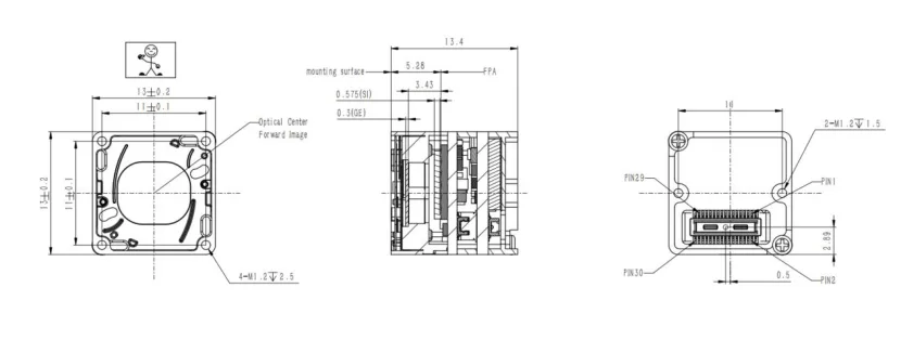
The CAMCUDA SuperMini 640 / 640T uses a 640×512 uncooled VOx detector with 8 µm pitch and ≤40 mK NETD at 25°C, F/1.0. The 640 is imaging-only at 50 Hz; the 640T is thermographic at 30 Hz. Published dimensions of 13 × 13 × 13.4 mm and weight below 3.5 g describe the bare core, excluding optics and boards. Its small package can reduce integration mass, but the lens, expansion board, regulated rails and host processing still belong in the full SWaP-C budget.
| Detector & Array Specifications | |
|---|---|
| Product Models | SuperMini 640: imaging-only | SuperMini 640T: thermographic |
| Detector Class & Resolution | Uncooled VOx LWIR | 640 × 512 pixels |
| Detector Pitch & Spectral Band | 8 µm | 8–14 µm |
| Model-Specific Frame Rate | 640: 50 Hz, no temperature measurement | 640T: 30 Hz |
| Optics & Mechanical Envelope | |
| Optical Path & Envelope | Confirm the selected lens and assembled FOV. Bare core: 13 × 13 × 13.4 mm, <3.5 g, excluding optics and boards. |
| Electrical, Physical & Environmental | |
| Voltage Rails & Power | MAIN_POWER 3.8–5.2 V plus +3.3 V and +1.8 V; follow power-on timing. Typical core power ≤0.5 W at 25°C, excluding expansion board. |
| Host Interface & Connector | 30-pin core interface; 1.8 V UART. CVBS requires an external buffer. Confirm MIPI/LVCMOS/USB implementation and model-specific data format. |
| Operating Temperature | −40°C to +70°C; thermography ambient specification −20°C to +60°C |
| Evaluation Hardware & Documents | Optional TMS6102V100F022 4-pin USB board; obtain the model-matched manual, board guide and host resources. AeroMini SDK resources are not SuperMini resources. |
Review SuperMini Configuration ➔
Product Showcase 2: CAMCUDA AeroMini 640 Lens-and-Tailboard Core
The CAMCUDA AeroMini 640 combines a 640×512 uncooled VOx detector, 12 µm pitch and ≤30 mK NETD at 25°C, F/1.0. The non-radiometric version is factory configured at 60 Hz by default or 30 Hz on request; it does not measure temperature. The 25 Hz radiometric version is available by enquiry. Select the lens and either the USB + CVBS + MIPI tailboard or the distinct Type-C + CVBS tailboard, then validate the supported host, format and rate for that assembly.
| Sensor Core Architecture | |
|---|---|
| Detector Type & Resolution | Uncooled VOx FPA | 640 × 512 pixels |
| Pixel Pitch & Spectral Band | 12 µm | 8–14 µm LWIR |
| Thermal Sensitivity (NETD) | ≤30 mK at 25°C, F/1.0 |
| Model-Specific Frame Rate | Non-radiometric: 60 Hz factory default / 30 Hz factory option. Radiometric: 25 Hz, availability enquiry. Output-path support requires confirmation. |
| Optics, Data & Evaluation | |
| Lens Selection | Use the current product configurator and confirm the ordered lens, FOV, focus and interface. The generic optics table above is not this product’s availability list. |
| Radiometric Configuration | 25 Hz version only; confirm measurement accuracy, calibration and available RAW/temperature format for the delivered firmware. |
| Mechanical Reference | 21 × 21 × 28 mm and <20 g exclude lens and flange; obtain configuration-matched complete assembly CAD. |
| Evaluation Resources | Official datasheet and product FAQ link to the user manual, serial commands and USB SDK resources. Match the board, firmware and host before integration. |
| Electrical, Mechanical & Interfaces | |
| Supply Voltage & Consumption | Board-dependent supply. Illustrated 16-pin POWER_IN1 and 26-pin POWER_IN2 are 5 V only; do not apply 12 V. Typical module power <0.5 W at 25°C; complete-kit power may differ. |
| Hardware Interface Support | USB + CVBS + MIPI and Type-C + CVBS are distinct tailboards. Confirm actual video modes, serial electrical levels and simultaneous-output support. |
| Weight & Operating Range | <20 g excluding lens and flange | −40°C to +80°C operating temperature |
Review AeroMini Configuration ➔
Consult the AeroMini datasheet and product FAQ for Linux drivers, examples and SDK resources. The linked package is configuration-specific; access to a resource does not establish host compatibility or an SDK test result. The four-page datasheet contains interface diagrams but no dimensioned assembly drawing. Request matched CAD for the selected lens and tailboard; the separate 7 mm STEP reference does not cover every assembly.
When sourcing OEM thermal hardware for regulated infrastructure projects, request configuration-specific origin, supplier and compliance documentation and have the applicable requirements reviewed. Our NDAA thermal camera module North America RFQ documents guide can support that documentation process; a product mention or a checklist does not establish legal compliance.
7. Edge AI Pipeline: Radiometric Processing with Embedded Frameworks
Plugging an uncooled thermal core into an embedded edge AI pipeline requires attention to the difference between thermal and visible imagery. A model trained on visible-spectrum datasets can perform poorly on thermal images without suitable adaptation, but its weights or architecture may still be useful. Define the input representation, train or fine-tune on representative thermal inspection data, and evaluate under the actual operating conditions.
Radiometric Pipeline Architecture for Edge Processors:
- ⚙️ Bit-Depth Quantization & Smart AGC: Confirm whether incoming values are raw counts, display intensities or calibrated temperature data. Choose scaling and quantization to match the model’s training pipeline. Fixed normalization, AGC, CLAHE or detail enhancement may suit different tasks; compare them on held-out inspection data. Preserve a separate calibrated data path for temperature measurement, because contrast enhancement changes intensity relationships.
- ⚙️ Input Representation & Fine-Tuning: A single-channel model, repeated grayscale channels or a defined pseudo-color mapping can each be evaluated; none is universally required or forbidden. Use the same representation during training and deployment, and test sensitivity to scene-dependent palettes or AGC. Frameworks such as PyTorch support adapting models, but conversion alone does not establish thermal-domain accuracy.
- ⚙️ Memory Transfers & Latency: On embedded Linux, DMA-BUF can share buffers between compatible capture and processing devices. A working low-copy path requires matching drivers, formats, strides, memory support and synchronization; conversion or CPU copies may still be necessary. Measure capture, queueing, preprocessing and inference times separately. Neither MIPI nor DMA-BUF guarantees an end-to-end latency below 20 ms. See the Linux V4L2 DMA-BUF requirements.
8. OEM Engineering RFQ & Host Board Integration Checklist
Before locking your schematic capture or releasing custom PCB tooling for your thermal enclosure, run through this final engineering checklist:
- ✅ Array Resolution & Frame Rate: Select the sampling and update rate for the inspection task. Lower-resolution sensors can reduce data and power demands, subject to the chosen hardware. For the featured families, distinguish SuperMini 640 imaging at 50 Hz from 640T thermography at 30 Hz, and AeroMini non-radiometric 60/30 Hz from radiometric 25 Hz by enquiry.
- ✅ Optics & Working Range: Check focal length, FOV, IFOV, focus and required feature size at the working distance. Confirm actual lens availability and assembled dimensions, and validate athermal performance across the agreed ambient range.
- ✅ Electrical Bus & Voltage Rails: Freeze the connector, board revision, physical mating orientation, electrical levels and power sequence. AeroMini 16/26-pin 5 V inputs, its Type-C tailboard and SuperMini’s multi-rail 30-pin core are distinct integrations.
- ✅ Chassis Thermal Path & Isolation: Follow the core’s mounting and heat-flow guidance. Stabilize its thermal environment while limiting unwanted heat from processors, motors and enclosure surfaces; validate drift and image quality during warm-up and ambient transitions.
- ✅ Driver Support & Bit-Depth: Validate the host driver, frame packing, controls and timestamps for the delivered firmware. RAW bit depth is not a Kelvin scale; temperature conversion applies only to a documented radiometric model and output mode.
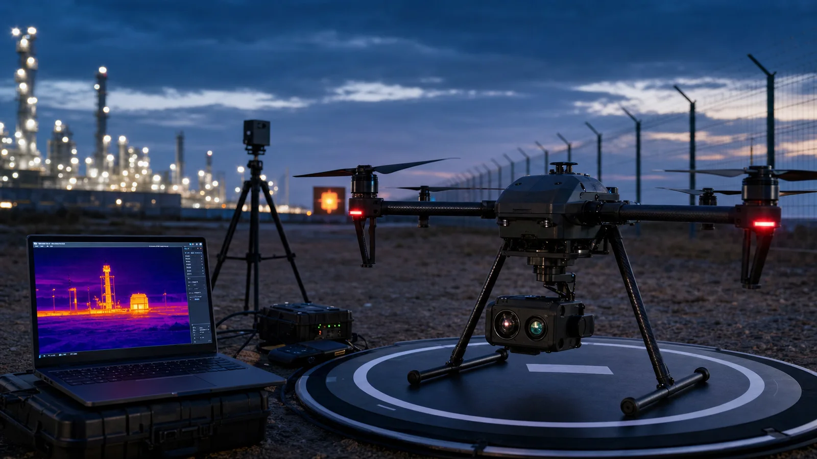
9. Frequently Asked Questions (OEM Engineering FAQ)
What is the primary technical difference between an active NIR camera and a passive thermal IR camera?
An active Near-Infrared (NIR) night-vision camera collects reflected illumination, commonly from 850 nm or 940 nm LEDs. Standard silicon CMOS detectors do not cover the full nominal NIR band; their useful response ends near 1.1 µm. Room-temperature objects emit very little thermal radiation in that region, so ordinary active NIR night vision does not provide temperature measurement. Ambient illumination can also contribute to a NIR image. A passive thermal IR camera in the 8–14 µm band detects thermal radiation and can form an image without visible light. Its signal can include both emitted and reflected radiation, with atmospheric effects along the path. Fog, rain, smoke and dust do not have a single universal transmission behavior. Temperature measurement requires a radiometric model, calibration and appropriate emissivity, reflected-temperature and environmental corrections; an imaging-only camera does not become radiometric simply because it operates in LWIR.
Why do OEM microbolometer modules require Non-Uniformity Correction (NUC) during field operation?
Uncooled microbolometer arrays contain many individual MEMS thermistor pixels above a silicon ROIC substrate. Fabrication variations cause differences in pixel response and offset. Internal temperature changes can also alter those offsets, producing fixed-pattern noise, striping and image drift. Factory NUC applies per-pixel correction terms, while field FFC can update offsets against a relatively uniform shutter reference. Some cores instead or additionally use temperature-model or scene-based shutterless compensation. Trigger behavior, interruption time and artifacts depend on the model, firmware and scene. NUC and FFC help maintain uniform imagery; they do not by themselves establish absolute temperature accuracy. Radiometric calibration and the measurement setup still need separate validation.
How should embedded engineers select between SPI, USB UVC, and MIPI CSI-2 interfaces for thermal cores?
Interface selection depends on the host architecture, available bandwidth, power budget, supported output format and measured latency.
SPI (Serial Peripheral Interface): A suitable lower-resolution sensor can stream to an MCU without a full operating system. Confirm the actual connector, rails, clock, packet format and calibrated-data support. SPI does not imply a particular power consumption, temperature format or 10-pin connector.
USB UVC: Often useful for bench evaluation and supported PC/SBC hosts. A compliant supported mode may use the standard video-class driver, while advanced controls or temperature data may need a separate SDK or interface. CDC serial, HID and vendor-specific endpoints are different; do not assume a virtual COM port or universal driverless compatibility.
MIPI CSI-2: Useful for a matched embedded receiver, but lane configuration, data type, packing, clocks, drivers and buffering must all be validated. MIPI does not guarantee a sub-20 ms pipeline. AeroMini’s USB + CVBS + MIPI and Type-C + CVBS tailboards need their respective wiring guides. SuperMini’s 30-pin multi-rail core interface is a separate design; neither the AeroMini pinout nor its SDK should be applied to it.
Why are standard optical glass lenses unusable for LWIR thermal IR camera modules?
Standard visible-light glasses such as BK7 and fused silica generally have insufficient transmission through the 8–14 µm band for LWIR lenses. Absorption and reflection depend on material, wavelength, thickness and surface treatment; a blanket “100% absorption” statement is misleading. Germanium is a common LWIR optical material with a refractive index near 4 around 10 µm. Its uncoated surfaces reflect strongly, so suitable anti-reflection coatings matter; DLC may also serve a protective role. Transmission must be checked for the actual coated element and assembled lens, rather than assuming a universal value above 92%. Moldable chalcogenide glass is another option, but transmission, cost and focus stability depend on composition and optical/mechanical design. Confirm system-level athermal performance across the specified operating range.
📚 References & Further Reading
- Inspection Guide: ASTM E1934-99a(2024) (inspection practice, not camera accuracy certification)
- Edge AI Framework: PyTorch
- Related Integration Guide: IR Camera Module Drone OEM Integration Checks
- Related Selection Guide: High-Resolution Thermal Imaging Camera OEM Selection Guide
- Related Compliance Guide: NDAA Thermal Camera Module North America RFQ Documents