Thermal Imaging Camera Price Breakdown: OEM Sensor & Module Cost Drivers
Thermal Imaging Camera Price Breakdown: OEM Sensor & Module Cost Drivers
If you have ever spent a late night on the bench trying to spec out a long-wave infrared (LWIR) payload for a drone gimbal, an autonomous rover, or a fixed factory-monitoring rig, you know how wild the pricing swings can be. You can browse online and find a tiny smartphone thermal dongle for $200, and five minutes later, you are staring down a formal quote for a ruggedized, SWaP-optimized OEM core that tops $5,000. It is easy to assume that spread is just marketing fluff or enterprise markup, but that is not what is happening on the shop floor. In the thermal imaging world, unit price comes down directly to semiconductor yields, vacuum packaging physics, optical raw materials, and the grueling labor hours required to calibrate pixels against physical blackbody furnaces.
Here’s the deal: evaluating the total cost of ownership (TCO) for an infrared module means looking past the initial unit sticker price. You have to evaluate the raw bill of materials (BOM), cleanroom wafer fabrication yields, optical manufacturing methods, and downstream digital signal processing (DSP) pipelines. When you are cramming thermal vision into a tight 13 mm enclosure, power dissipation, pixel pitch, and radiometric calibration will either make or break your hardware architecture and engineering budget. Look, cutting corners on the front-end sensor almost always backfires in the form of massive firmware workarounds or field failures down the road. Let’s break down the actual technical and economic mechanics that dictate what an uncooled thermal camera core costs.
Table of Contents
- 👉 1. Microbolometer FPA Architecture & Semiconductor Economics
- 👉 2. LWIR Optics Mechanics: Germanium vs. Chalcogenide Glass & Athermalization
- 👉 3. Image Processing Pipelines & Radiometric Calibration Overheads
- 👉 4. SWaP-C Optimization & Environmental Reliability Screening
- 👉 5. Comprehensive OEM Product Showcase & Engineering Analysis
- 👉 6. OEM Thermal Module Engineering Benchmark & Spec Matrix
- 👉 7. Interface Topologies & Systems Integration (MIPI, USB, RS-422)
- 👉 8. B2B Thermal Imaging Camera Price Tiers & Volume Sourcing Strategy
- 👉 9. Comprehensive OEM Engineering FAQs
- 👉 10. Conclusion & Strategic System Specification Checklist
1. Microbolometer FPA Architecture & Semiconductor Economics
The focal plane array (FPA) is the beating heart of an uncooled long-wave infrared camera module. In almost every hardware build, the raw sensor represents between 45% and 65% of the total component BOM. If you want to understand why thermal cores are priced the way they are, you have to look at thin-film materials, lithography scaling, cleanroom yields, and the packaging processes needed to seal microbridges in a hard vacuum.
Vanadium Oxide (VOx) vs. Amorphous Silicon (a-Si)
The thin-film material deposited on the microbolometer’s suspended microbridge structures directly dictates both the thermal sensitivity and the manufacturing yield:
- ⚙️ Vanadium Oxide (VOx): This is the uncontested gold standard for defense, industrial UAV payloads, and precision instrumentation. VOx delivers a high temperature coefficient of resistance (TCR ≈ 2% to 3% per Kelvin) alongside exceptionally low intrinsic 1/f flicker noise. This allows VOx cores to easily achieve a Noise Equivalent Temperature Difference (NETD) of ≤40 mK or even ≤30 mK at F1.0, pulling crisp contrast out of low-gradient scenes. The trade-off is in the fab: depositing uniform, stoichiometric VOx thin films requires specialized MEMS foundry equipment, keeping the baseline silicon cost higher than standard CMOS runs.
- ⚙️ Amorphous Silicon (a-Si): Built directly on standard commercial silicon CMOS lines. While a-Si benefits from mature lithography and high raw wafer volumes, it suffers from lower TCR and substantially higher 1/f noise. In the field, an a-Si detector typically sits at a sluggish 50 mK to 80 mK NETD and drifts significantly when ambient temperatures swing, requiring more frequent calibration shutter cycles.
For an in-depth review of thermal sensor physical operational principles, refer to the Wikipedia Microbolometer reference.
Pixel Pitch Scaling: 17 µm vs. 12 µm vs. 8 µm
Pixel pitch—the physical distance from the center of one microbolometer pixel to the center of the next—drives die size, wafer yields, and the physical mass of the optics sitting in front of the array:
- ⚙️ 17 µm Architecture: The legacy industrial standard. A 640 × 512 array at 17 µm requires an active sensor area of roughly 10.88 mm × 8.70 mm. That massive footprint yields very few pristine dies per 8-inch silicon wafer and demands bulky, heavy Germanium lenses with wide clear apertures, which drives up payload weight and material costs.
- ⚙️ 12 µm Architecture: The current workhorse standard for professional OEM modules, as seen on the CAMCUDA AeroMini 640. Shrinking the 640 × 512 active area to 7.68 mm × 6.14 mm strikes a sweet spot between photon collection efficiency, compact lens barrels, and cleanroom wafer yield.
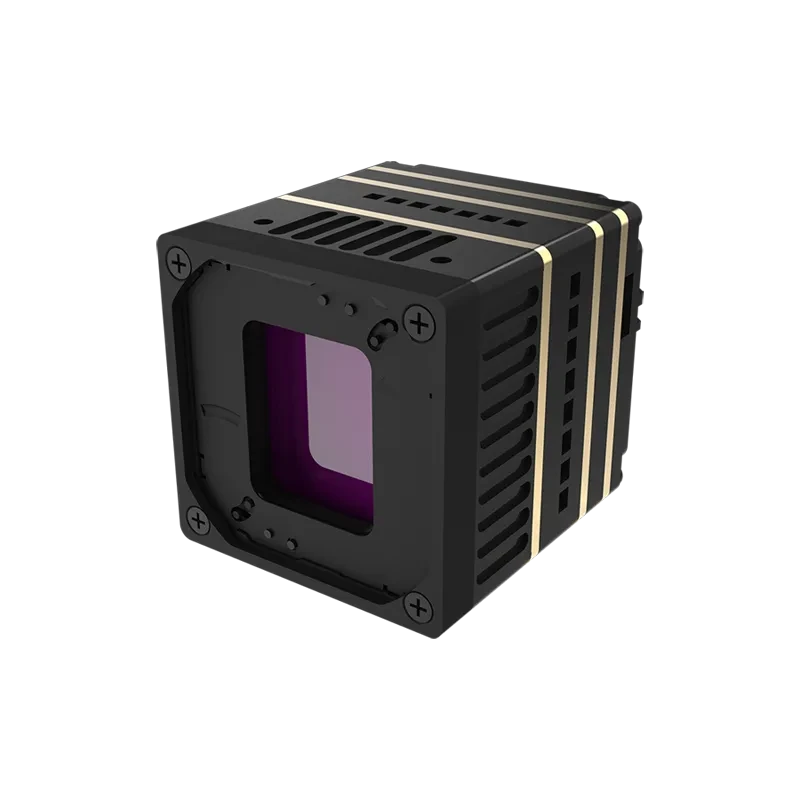
- ⚙️ 8 µm Architecture: The bleeding edge of commercial microbolometer engineering, featured on modules like the CAMCUDA SuperMini 640. Reducing pixel pitch down to 8 µm collapses that 640 × 512 active area to just 5.12 mm × 4.10 mm. This more than doubles the net usable die count per processed wafer, slashing base detector fabrication costs while enabling pocket-sized 13 mm × 13 mm core envelopes and lightweight, short-focal-length optics.
Packaging Topologies: Metal Can vs. Ceramic vs. Wafer-Level Packaging (WLP)
Because microbolometers measure microscopic temperature changes in delicate suspended bridges, those bridges must live in a permanent high-vacuum envelope (<10-2 Pa). If air leaks in, ambient gas molecules conduct heat away, blinding the sensor. How that vacuum is built determines a huge chunk of module assembly cost:
- ⚙️ Ceramic & Metal Hermetic Packages: Traditional assemblies use discrete ceramic or Kovar metal cans fitted with non-evaporable getters (NEG) that get baked and activated at high temperatures. Every unit is sealed individually and leak-tested manually, adding $150 to $350 per detector in pure packaging overhead.
- ⚙️ Wafer-Level Packaging (WLP): An etched silicon or Germanium cap wafer coated with anti-reflective treatments is bonded directly to the detector wafer in an automated high-vacuum chamber before dicing. WLP seals hundreds of microbolometers simultaneously in one single manufacturing run. This cuts discrete manual labor to zero, shrinks total module mass down below 3.5 grams, and enables competitive pricing at high volumes.
2. LWIR Optics Mechanics: Germanium vs. Chalcogenide Glass & Athermalization
Standard optical glass like BK7 or fused silica is essentially an opaque wall to infrared light between 8 µm and 14 µm. You cannot use normal camera glass; you must use specialized infrared-transmitting materials. In almost every thermal build, the optical barrel accounts for 25% to 40% of the complete core BOM.
Monocrystalline Germanium (Ge) Optics
Monocrystalline optical-grade Germanium is the undisputed king of thermal transmission. It features a sky-high refractive index (n ≈ 4.002 at 10 µm) and low chromatic dispersion, which lets optical designers construct ultra-fast F1.0 to F1.1 lenses using minimal optical elements. But raw Germanium is an expensive, geopolitically sensitive raw material. You cannot mold it in a press; it has to be turned on single-point diamond turning (SPDT) lathes or ground on precision CNC polishing benches, then coated with multi-layer anti-reflective (AR) or diamond-like carbon (DLC) coatings. A narrow-field telephoto Germanium lens can easily exceed the cost of the sensor core itself.
Chalcogenide Glass & Precision Glass Molding (PGM)
When high-volume production demands lower BOM costs, optical engineers turn to chalcogenide glasses—amorphous compounds synthesized from sulfur, selenium, or tellurium (such as Ge28Sb12Se60 or As40Se60). Unlike crystalline Germanium, chalcogenide glass softens at manageable temperatures, making it compatible with Precision Glass Molding (PGM) in polished tungsten-carbide dies. Once tooling is paid for, PGM eliminates manual diamond turning and slashes optic production costs by 50% to 70% at volumes above 5,000 units. The catch? Chalcogenide has a lower refractive index (n ≈ 2.5 to 2.8), which means hitting an F1.0 aperture often requires thicker, multi-element optical designs.
Mechanical Athermalization: Passive vs. Active
Germanium suffers from an extreme thermal-optic coefficient (dn/dT ≈ 396 × 10-6 K-1). In plain English: when the ambient temperature changes, the lens’s refractive index drifts rapidly. An optic focused sharply at room temperature (+25°C) will blur into an unusable mess at -20°C or +60°C unless compensated for.
- ⚙️ Passive Mechanical Athermalization: The lens barrel combines materials with contrasting coefficients of thermal expansion (aluminum, stainless steel, and specialized engineering plastics). As temperature shifts and expands the Germanium elements, the mechanical barrel expands or contracts in the opposite direction, physically holding the focal spot locked on the FPA plane without drawing a single milliamp of electrical power.
- ⚙️ Active Electromechanical Athermalization: Uses an integrated stepper motor or voice-coil actuator driven by firmware lookup tables tied to internal thermistors. While this provides razor-sharp focus across extreme operating envelopes, it adds moving mechanical parts, weight, power draw, and additional failure modes.
For more details on matching optical configurations with UAV payload constraints, consult our technical guide on choosing a 640×512 thermal camera module for drone payloads.
3. Image Processing Pipelines & Radiometric Calibration Overheads
Raw output coming off a microbolometer array looks like static noise. Every individual microbridge pixel has slight manufacturing variations in resting electrical resistance, thermal responsiveness, and temporal noise. Turning those microvolt-level signals into crisp video requires dedicated FPGA or ASIC signal processing and disciplined thermal calibration.
Real-Time Hardware Image Processing Pipelines
Modern OEM cores process 640 × 512 raw data frames at 30 Hz to 50 Hz with sub-frame latency. A complete hardware image processing pipeline handles several crucial jobs:
- ⚙️ Non-Uniformity Correction (NUC): Normalizes gain and offset across all 327,680 individual pixels. Advanced modern modules employ shutterless scene-based NUC (SBNUC) algorithms, preventing annoying video freeze frames during dynamic flight or surveillance operations.
- ⚙️ Bad Pixel Replacement (BPR): Maps dead or noisy pixels on the fly, interpolating their values using spatial neighborhood filtering so the user never sees dead spots.
- ⚙️ Digital Detail Enhancement (DDE): Applies high-pass spatial filtering to pull faint edge details and object outlines out of low-contrast thermal backgrounds.
- ⚙️ 3D Noise Reduction (3D-NR): Blends spatial filtering within a frame and temporal filtering across consecutive frames to lower the noise floor without introducing motion smear.
The Radiometric Calibration Cost Premium
There is a massive price gap between a core that outputs a pretty visual picture and one that acts as a calibrated scientific pyrometer:
- ✅ Standard Imaging Cores (e.g., CAMCUDA SuperMini 640): Tuned purely for thermal contrast, visual clarity, and target identification. ADC counts are converted straight into dynamic grayscale or pseudo-color palettes (White Hot, Black Hot, Rainbow) for human eyes or machine vision classifiers.
- ✅ Radiometric/Thermographic Cores (e.g., CAMCUDA SuperMini 640T): Calibrated to report the exact temperature of every single pixel in the frame. Achieving this requires rigorous factory overhead:
- Environmental Chamber Soaking: Batches of modules sit in automated environmental chambers running through their entire temperature spec (-20°C to +60°C ambient) while staring into precision cavity blackbody radiators set from -20°C up to +650°C.
- Pixel-by-Pixel Polynomial LUT Generation: The automated rig builds high-order polynomial correction curves for every individual pixel, burning those custom lookup tables straight into onboard non-volatile flash.
- Real-Time Environmental Math: Firmware continuously polls onboard thermistors and recalculates temperature outputs in real time, factoring in user parameters like target distance, emissivity, and ambient humidity.
That multi-hour blackbody calibration process is a major factory bottleneck, which is why true radiometric cores routinely command a 20% to 40% price premium over imaging-only models.
4. SWaP-C Optimization & Environmental Reliability Screening
In aerospace, tactical defense, and industrial automation, Size, Weight, Power, and Cost (SWaP-C) dictate engineering decisions. Shaving grams and millimeters while preserving industrial reliability requires high-density circuit layout, specialized structural alloys, and extensive screening.
Physical Miniaturization and High-Density Interconnects
Packing a complete 640 × 512 LWIR core into a 13 mm × 13 mm footprint that weighs under 3.5 grams requires multi-layer rigid-flex printed circuit boards, micro-pitch ball grid arrays (BGAs), and CNC-machined magnesium or aviation-grade aluminum housings. Assembling boards this dense demands automated high-precision pick-and-place gear, active optical alignment stations, and specialized capillary underfill to prevent solder fatigue under thermal cycling.
Thermal Dissipation & Parasitic Noise Control
Microbolometers detect fractions of a degree in temperature variation, meaning internal heat generated by onboard FPGAs, microcontrollers, and switching power stages can easily degrade the sensor’s own readouts. High-efficiency cores are designed to draw ≤0.5 W of typical power (such as the CAMCUDA SuperMini 640). Keeping power consumption that low prevents heat from bleeding into the FPA, eliminates the need for bulky copper heatsinks or active cooling fans, and maximizes battery life on portable systems.
Industrial Environmental Screening & Stress Qualification
Industrial thermal modules are built to operate reliably in harsh, demanding environments, undergoing extensive stress qualification:
- ⚙️ Operating Temperatures: Stable performance from -40°C to +85°C without image degradation or optical defocusing.
- ⚙️ Mechanical Shock: Tested to withstand high mechanical shocks of 80 g @ 4 ms across all 3 axes and 6 directions.
- ⚙️ Random Vibration: Built to endure 6.06 g random vibration profiles across all structural axes, ensuring durability in high-vibration drone airframes and industrial machinery.
5. Comprehensive OEM Product Showcase & Engineering Analysis
To examine how these engineering and pricing factors apply in practice, let us analyze two production-ready uncooled LWIR camera cores designed for UAV payloads, robotics, and industrial integration.
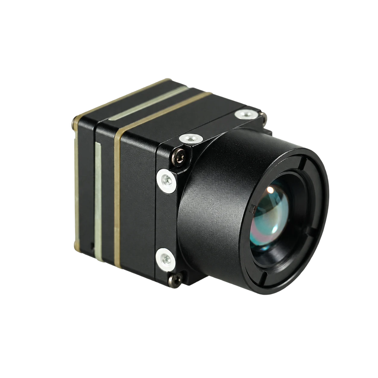
CAMCUDA AeroMini 640 LWIR Thermal Camera Core
CAMCUDA AeroMini 640 combines a 640 × 512 uncooled VOx detector with 12 μm pixels for UAV payload and OEM integration. The non-radiometric version uses a 60 Hz factory default, with 30 Hz available as a factory option. The separate radiometric version operates at 25 Hz. Select the lens and interface board for the required host and output path. Published dimensions are 21 × 21 × 28 mm and weight is below 20 g, excluding lenses and flanges. Non-radiometric imaging does not provide calibrated temperature readings.
Key Architectural Specifications
| Detector Type | Vanadium oxide (VOx) uncooled infrared detector |
|---|---|
| Resolution & Pixel Pitch | 640 × 512 | 12 μm |
| Detector Frame Rate | Non-radiometric: 60 Hz factory default; optional 30 Hz factory configuration. Radiometric: 25 Hz. |
| Spectral Band & NETD | 8–14 μm | ≤30 mK at 25 °C, F/1.0 |
| Image Processing | NUC/FFC settings are configurable through supported PC software; confirm supported behavior for the operating environment and firmware. |
| Image Adjustments | Configuration-dependent; confirm the supported controls for the selected firmware. |
| Pseudo Color Palettes | White hot / Black hot |
| Supply Voltage & Power | Board-dependent input; illustrated POWER_IN1 / POWER_IN2 pins: 5 V only. Typical module power: <0.5 W at 25 °C; complete-kit consumption may differ. |
| Video & Control Interfaces | Interface options include USB + CVBS + MIPI or Type-C + CVBS. UART, RS232 and RS422 availability depends on the selected board. Confirm output path, firmware and host compatibility. |
| Dimensions & Weight | 21 × 21 × 28 mm | <20 g, excluding lenses and flanges |
| Operating / Storage Temp | −40 °C to +80 °C | −50 °C to +85 °C |
| Vibration & Shock | Qualification data must be confirmed for the selected assembly. |
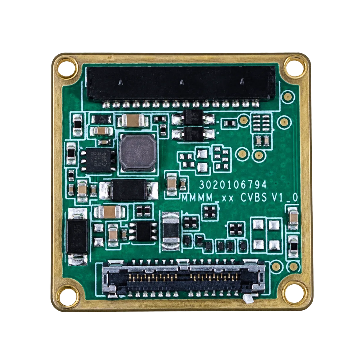
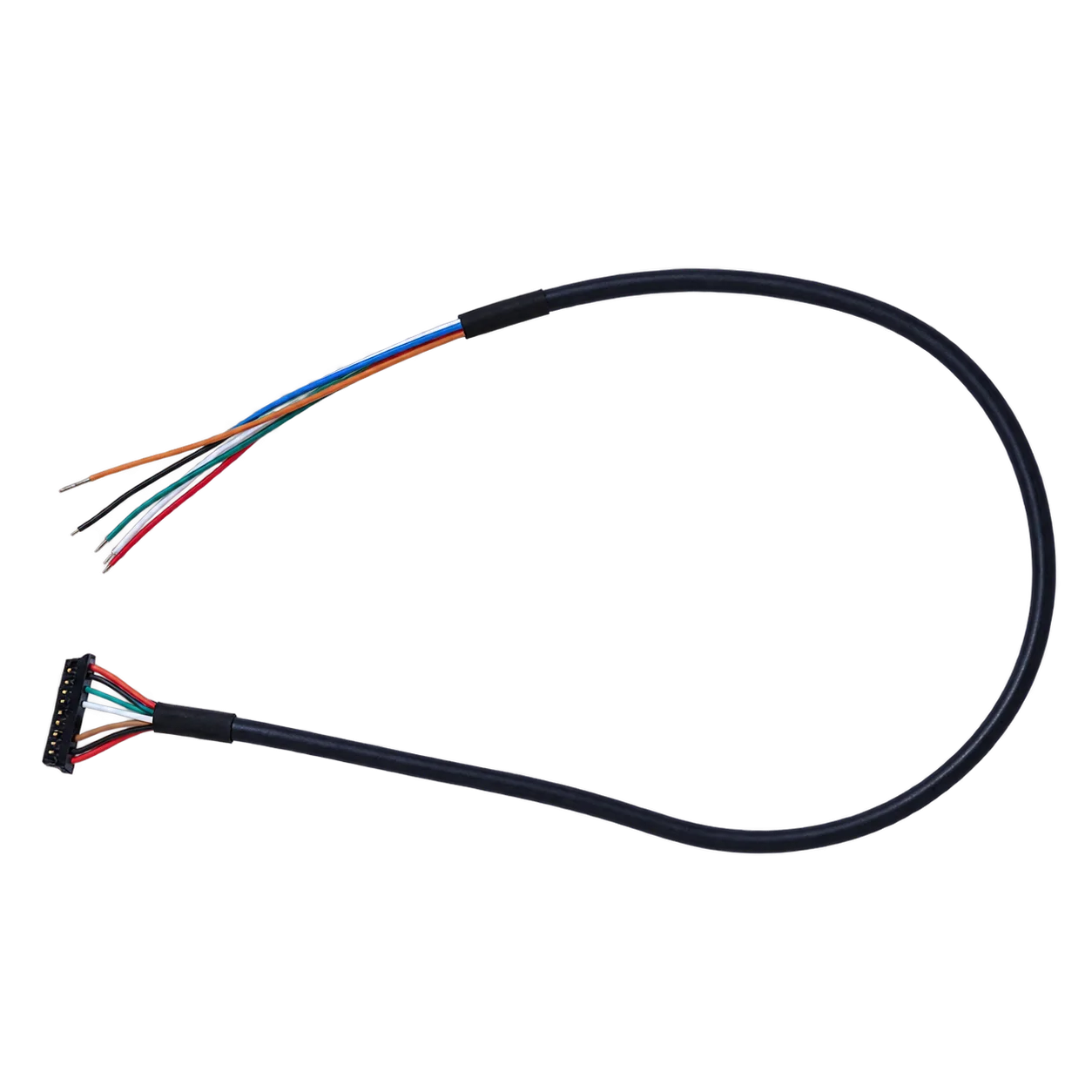
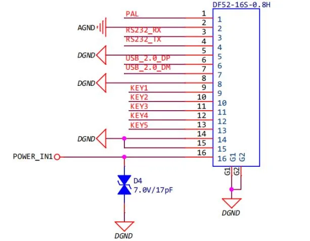
For the matching connector layout, complete signal assignments and 26-pin MIPI/DVP reference, use the complete AeroMini datasheet and original 16-pin signal table. Do not apply 12 V to POWER_IN1 or POWER_IN2, infer wire functions from colors, or reuse these diagrams for the Type-C board.
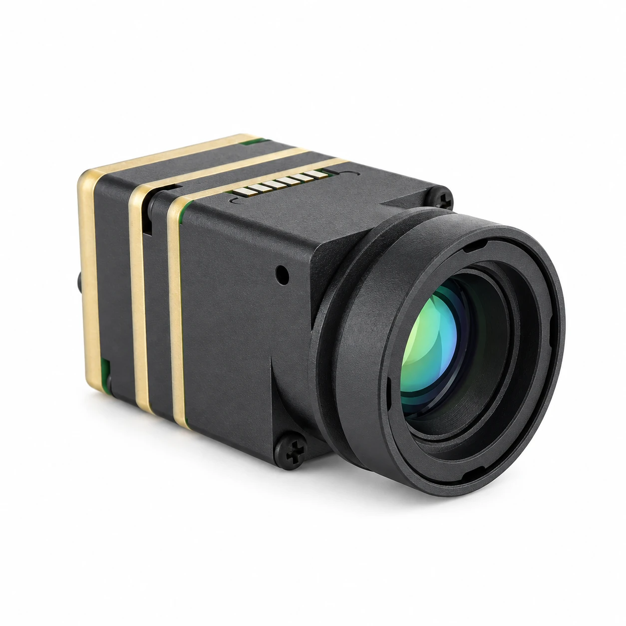
CAMCUDA SuperMini 640 / 640T Ultra-Light LWIR Thermal Module
The CAMCUDA SuperMini 640 / 640T series combines a 640 × 512 uncooled VOx detector with an advanced 8 µm pixel pitch into an ultra-compact 13 mm × 13 mm footprint weighing under 3.5 grams. Engineered for low-SWaP micro-drones, lightweight gimbals, FPV systems, and embedded edge devices, it consumes ≤0.5 W of power. It is available in two factory-configured versions: the high-speed 50 Hz imaging-only CAMCUDA SuperMini 640 and the 30 Hz radiometric CAMCUDA SuperMini 640T with calibrated temperature measurement.
Factory Model Variations
- ✅ CAMCUDA SuperMini 640 (Imaging Only): 50 Hz frame rate; 8-bit LVCMOS / BT656 and 2-lane MIPI interfaces; designed for low-latency visual observation and drone navigation.
- ✅ CAMCUDA SuperMini 640T (Thermographic): 30 Hz frame rate; CDS3 and MIPI temperature-data paths; dual measurement ranges of -20°C to +150°C and 100°C to +650°C for industrial inspection and monitoring.
Athermalized F1.0 Lens Options
| Focal Length | Field of View (H × V) | Aperture | IFOV |
|---|---|---|---|
| 3.7 mm | 90.0° × 68.2° | F1.0 | 2.16 mrad |
| 6.1 mm | 46.6° × 37.6° | F1.0 | 1.31 mrad |
| 8.7 mm | 40.0° × 32.2° | F1.0 | 0.92 mrad |
| 11 mm | 24.9° × 20.0° | F1.0 | 0.73 mrad |
Electrical & Signal Interface Details (Hirose DF40C-30DP-0.4V(51))
| Interface Rail | Voltage / Spec | Integration Note |
|---|---|---|
| MAIN_POWER | 3.8–5.2 V (Typical 5 V) | 10 mV p-p maximum noise |
| +3.3 V rail | 3.28–3.32 V | 10 mV p-p maximum noise |
| +1.8 V rail | 1.78–1.82 V | 1 mV RMS, 1 Hz–50 kHz low-noise requirement |
| Digital Video | 8-bit LVCMOS; 2-lane MIPI | 640 uses BT656; 640T uses CDS3 format |
| Control / Comm | UART (1.8 V logic) | TX/RX defined from core; expansion board TMS6102V100F022 adds USB |
For the SuperMini core without an expansion board, consult the complete SuperMini manual: 30-pin orientation and pin table, PDF pages 6–7. The bare-core mechanical drawing, PDF page 13 excludes the lens and expansion board. These references do not define an optional USB-board or Type-C cable pinout.
6. OEM Thermal Module Engineering Benchmark & Spec Matrix
The matrix below compares the structural, optical, electrical, and thermal parameters of the CAMCUDA AeroMini 640 and CAMCUDA SuperMini 640 / 640T, highlighting how different design architectures align with specific application requirements.
| Engineering Parameter | CAMCUDA AeroMini 640 | CAMCUDA SuperMini 640 / 640T |
|---|---|---|
| Detector Architecture | VOx uncooled FPA | Vanadium Oxide (VOx) Uncooled FPA |
| Array Resolution | 640 × 512 pixels | 640 × 512 pixels |
| Pixel Pitch | 12 μm | 8 μm (Ultra-High Density) |
| Detector Frame Rate | Non-radiometric: 60 Hz default / 30 Hz factory option; radiometric: 25 Hz | 640: 50 Hz | 640T: 30 Hz |
| Thermal Sensitivity (NETD) | ≤30 mK at 25 °C, F/1.0 | ≤40 mK @ 25°C, F1.0 |
| Core Weight (Bare) | <20 g, excluding lenses and flanges | <3.5 g |
| Dimensions (W × H × D) | 21 × 21 × 28 mm, excluding lenses and flanges | 13 mm × 13 mm × 13.4 mm |
| Power Consumption | <0.5 W typical module power at 25 °C; complete-kit consumption may differ | ≤0.5 W (Typical Core) |
| Digital Video Output | USB, MIPI and BT.656 paths depend on board/firmware; confirm the selected configuration | 8-bit LVCMOS / BT656, 2-lane MIPI |
| Control Interface | UART / RS232 / RS422, board-dependent | UART (1.8 V logic) / 30-Pin DF40C |
| Thermography Support | Non-radiometric: none; radiometric: −20 °C to +550 °C at 25 Hz | 640: None | 640T: -20°C to +650°C |
| Operating Temperature | −40 °C to +80 °C | -40°C to +85°C |
7. Interface Topologies & Systems Integration (MIPI, USB, RS-422)
Your choice of electrical interface ripples straight into your carrier board layout, host processor overhead, and overall BOM cost. Getting this wrong means burning budget on unnecessary bridge chips or fighting latency issues on the flight line.
Direct Embedded Sensor Buses: MIPI CSI-2 & BT.656
When you are building a custom embedded vision system powered by an NVIDIA Jetson Orin, NXP i.MX8, or Qualcomm robotics SoC, direct low-level buses are the way to go:
- ⚙️ MIPI CSI-2 (2-Lane): Streams raw 14-bit radiometric data or processed 8-bit frames straight into the host processor’s hardware image signal processor (ISP). This bypasses USB PHY controllers and intermediate bridge chips, keeping pipeline latency well below 10 ms.
- ⚙️ BT.656 / 8-bit LVCMOS: A standard parallel digital bus that interfaces smoothly with hardware video encoders and FPGAs. It uses simple clocking schemes and skips the driver baggage of USB stacks.
For more integration guidelines, review our checklist on thermal camera core selection and interface integration.
Standard Industrial Plug-and-Play: USB 2.0 & RS-422
If you are integrating onto an industrial single-board computer (SBC) or want to get a prototype working quickly on a Linux or Windows laptop, standardized buses save hundreds of engineering hours:
- ✅ USB Video Class (UVC): Turns the thermal core into a driverless, plug-and-play video capture node compatible with standard OpenCV, ROS, and V4L2 pipelines out of the box.
- ✅ RS-422 Serial Communication: Employs differential signaling to shrug off heavy electromagnetic interference (EMI) kicked off by nearby drone ESCs and high-current industrial motors, allowing reliable control over long cable runs.
For official USB implementation specifications, refer to the USB-IF Document Library.
Power Rail Noise and Ripple Filtering
Uncooled microbolometer Read-Out Integrated Circuits (ROICs) measure microvolt-level charge fluctuations. If your power supply has switching noise or ripple, it will show up directly on screen as horizontal banding or rolling lines. When you drop a module like the CAMCUDA SuperMini 640 onto a carrier board, your +3.3 V and +1.8 V rails must hold ripple below 10 mV peak-to-peak, with high-frequency noise limited to <1 mV RMS. In the shop, this means running multi-stage low-dropout linear regulators (LDOs) and dedicated LC filtering ferrite beads right next to the Hirose connector.
8. B2B Thermal Imaging Camera Price Tiers & Volume Sourcing Strategy
Thermal camera core pricing follows clear, predictable tiers dictated by sensor resolution, manufacturing volumes, optical specs, and radiometric calibration demands. Here is where the actual OEM market sits today across commercial volume brackets:
| Resolution | Pixel Pitch | Target Market & Features | 1–9 Units (Sample) | 1,000+ Units (OEM) |
|---|---|---|---|---|
| 256 × 192 | 12 μm | Entry-level IoT, handheld test tools | $180 – $350 | $65 – $120 |
| 384 × 288 | 12 μm | Mid-tier industrial inspection, security cameras | $450 – $800 | $220 – $380 |
| 640 × 512 | 12 μm / 8 μm | Standard OEM drone payloads, robotics vision | $900 – $1,800 | $450 – $750 |
| 640 × 512 (Radiometric) | 12 μm / 8 μm | Precision thermal analysis, utility grid inspection | $1,400 – $2,600 | $700 – $1,200 |
| 1280 × 1024 (HD) | 10 μm / 12 μm | High-altitude aerospace, long-range defense ISR | $4,500 – $9,000 | $2,500 – $4,500 |
Practical Procurement Tactics
- ✅ Leverage Volume Scaling: Committing to scheduled production batches of 100, 500, or 1,000 units drops per-unit prices by 40% to 60% compared to prototype samples. This amortizes chamber setup time and automated optical alignment across high-throughput runs.
- ✅ Stick to Standard Catalog Lenses: Custom diamond-turned optical focal lengths carry steep NRE tooling charges. Choosing standard catalog athermalized optics (like 3.7 mm, 6.1 mm, 8.7 mm, or 11 mm) keeps your budget intact.
- ✅ Check Dual-Use Export Classifications: Always verify supplier NDAA compliance and confirm whether high-framerate 50 Hz configurations require specific export licensing for your deployment territories.
For more sourcing guidance, visit the CAMCUDA Support and FAQ Knowledge Base.
9. Comprehensive OEM Engineering FAQs
Why is there a large price difference between consumer thermal gadgets and professional OEM camera cores?
What specific hardware components drive the bill of materials (BOM) cost of an uncooled LWIR core?
1. The Microbolometer Focal Plane Array (45% to 65% of BOM): The biggest cost driver, determined by pixel pitch (8 µm vs. 12 µm), thin-film material (VOx vs. a-Si), MEMS wafer yield, and Wafer-Level Packaging (WLP) efficiency.
2. Infrared Optical Elements (25% to 40% of BOM): Monocrystalline Germanium blanks require precision single-point diamond turning (SPDT), anti-reflective coatings, and passive mechanical athermalization barrels to stay focused across temperature swings.
3. Embedded Signal Processing: Low-power FPGAs or ASICs running real-time non-uniformity correction (NUC), bad pixel interpolation, and digital detail enhancement (DDE) at 50 Hz.
4. Factory Calibration & Screening Overhead: Multi-point blackbody calibration runs and stress screening (thermal cycling, 6.06 g vibration, and 80 g shock testing) tie up specialized chamber equipment and add labor time to every finished unit.
Why do radiometric (temperature-measuring) thermal modules cost more than imaging-only cores?
How does transitioning from a 12 µm to an 8 µm pixel pitch affect module dimensions and unit price?
10. Conclusion & Strategic System Specification Checklist
When you are architecting a vision subsystem and budgeting for long-wave infrared hardware, look at the entire operational picture rather than chasing sensor resolution alone. Sourcing the right module means balancing pixel pitch scaling, optical barrel mechanics, bus bandwidth, power limits, and radiometric calibration requirements against your commercial target BOM.
Before locking in your component specs and issuing an RFQ, run through this hardware checklist:
- ⚙️ Define the Core Mission: Determine if your software stack actually needs absolute radiometric temperature values (industrial utility audit, fire spot detection) or high-contrast visual video (drone piloting, target tracking, ISR).
- ⚙️ Lock Down SWaP Envelope: For micro-gimbals and battery-sensitive airborne systems, spec ultra-lightweight 8 µm architectures like the CAMCUDA SuperMini 640 (<3.5 g, ≤0.5 W) to extend flight endurance and reduce payload inertia.
- ⚙️ Match Electrical Interfaces: For AeroMini 640, select the interface board and confirm the required USB, MIPI or CVBS output, control connection and host compatibility before ordering. Include cable assembly, board revision and power requirements in the integration review.
- ⚙️ Standardize Optics Early: Align your required field of view with standardized off-the-shelf athermalized lenses (3.7 mm, 6.1 mm, 8.7 mm, 11 mm) to eliminate custom diamond-turning NRE charges.
📚 References & Further Reading
- Industry Standard: Wikipedia – Microbolometer Physics and Operating Principles
- Industry Standard: USB-IF Document Library – USB Video Class (UVC) Specifications
- Related Guide: Thermal Camera Core Selection: Interface, Resolution, and Integration Checklist
- Related Guide: How to Choose a 640×512 Thermal Camera Module for Drone Payloads
- Support Knowledge Base: CAMCUDA OEM Core Integration & Technical Sourcing FAQ