Thermal Imager Camera Integration Guide: Selecting OEM Cores for UAV and Industrial Systems
Thermal Imager Camera Integration Guide: Selecting OEM Cores for UAV and Industrial Systems
Integrating a high-performance thermal imager camera into modern unmanned aerial vehicles (UAVs), autonomous mobile robots (AMRs), automated security gimbals, and industrial machine vision platforms means dealing with tough electro-optical, thermal, mechanical, and compute trade-offs. Here’s the deal: unlike standard visible-spectrum sensors that simply capture reflected ambient light, a thermal imager camera operates by detecting raw long-wave infrared (LWIR) blackbody radiation emitted directly by real-world targets. Embedding an uncooled LWIR OEM module into an autonomous payload requires hardware engineers and systems architects to carefully balance Size, Weight, Power, and Cost (SWaP-C), microbolometer material physics, infrared optical transmission windows, digital video streaming interfaces, and real-time edge processing architectures.
Look, pick the wrong sensor core or a mismatched focal length, and you will run into nasty operational failures out in the field. We are talking excessive thermal baseline drift, massive video pipeline latency, shutter-induced tracking dropouts, severe optical vignetting, and washed-out target detail. This technical guide breaks down the component-level engineering required to evaluate, integrate, and deploy OEM thermal camera cores without cutting corners. By diving into uncooled Vanadium Oxide (VOx) focal plane arrays, calculating spatial resolution using the Johnson criteria, assessing embedded digital transport buses like MIPI CSI-2, USB Video Class (UVC), and CVBS, and walking through production modules—from ultralight 23.1 g standalone cores to 4 TOPS dual-spectrum edge-AI platforms—engineers can streamline board spins and avoid painful hardware redesigns.
Table of Contents
- 👉 1. LWIR Sensor Physics & Microbolometer Core Architecture
- 👉 2. Optical Selection, IFOV Calculations, and Johnson Criteria
- 👉 3. Video Interfaces, Latency, and Power Architecture (MIPI, UVC, CVBS)
- 👉 4. OEM Product Hardware Showcase & Technical Comparison
- 👉 5. Dual-Spectrum Sensor Fusion & Edge-AI Tracking Implementation
- 👉 6. Thermal Dissipation, Shutter Calibration (NUC), and Mechanical Mounting
- 👉 7. Comprehensive Industrial Engineering FAQ
1. LWIR Sensor Physics & Microbolometer Core Architecture
Every OEM thermal imaging camera functions as an electromagnetic radiation transducer operating across the Long-Wave Infrared (LWIR) atmospheric transmission window, spanning the 8 µm to 14 µm spectral band. Governed by Planck’s Radiation Law and the Stefan-Boltzmann Law, all physical matter with a thermodynamic temperature above absolute zero (0 Kelvin) emits thermal radiation directly proportional to its surface temperature and spectral emissivity. Because terrestrial targets—such as personnel, vehicle drivetrains, electrical utility substations, and civil infrastructure—emit heavily within this 8–14 µm band across common operating temperatures from -40°C to +150°C, an uncooled microbolometer sensor array detects these emitted photon streams directly without requiring bulky cryogenic cooling engines or active illumination.
The structural foundation of an uncooled thermal imager camera is the Focal Plane Array (FPA). An uncooled FPA consists of a two-dimensional matrix of micromachined bolometer pixels suspended above a silicon substrate via micro-bridge thermal isolation legs. Each individual pixel membrane absorbs incoming infrared photons, causing a minute localized temperature increase. This thermal rise alters the electrical resistance of the thin-film detector material. A Readout Integrated Circuit (ROIC) bonded beneath the microbolometer matrix measures these resistance shifts through row-column multiplexing, converts the analog electrical signals into raw digital frame data using high-precision onboard Analog-to-Digital Converters (ADCs), and streams the uncompressed payload directly to the core’s Digital Signal Processor (DSP).
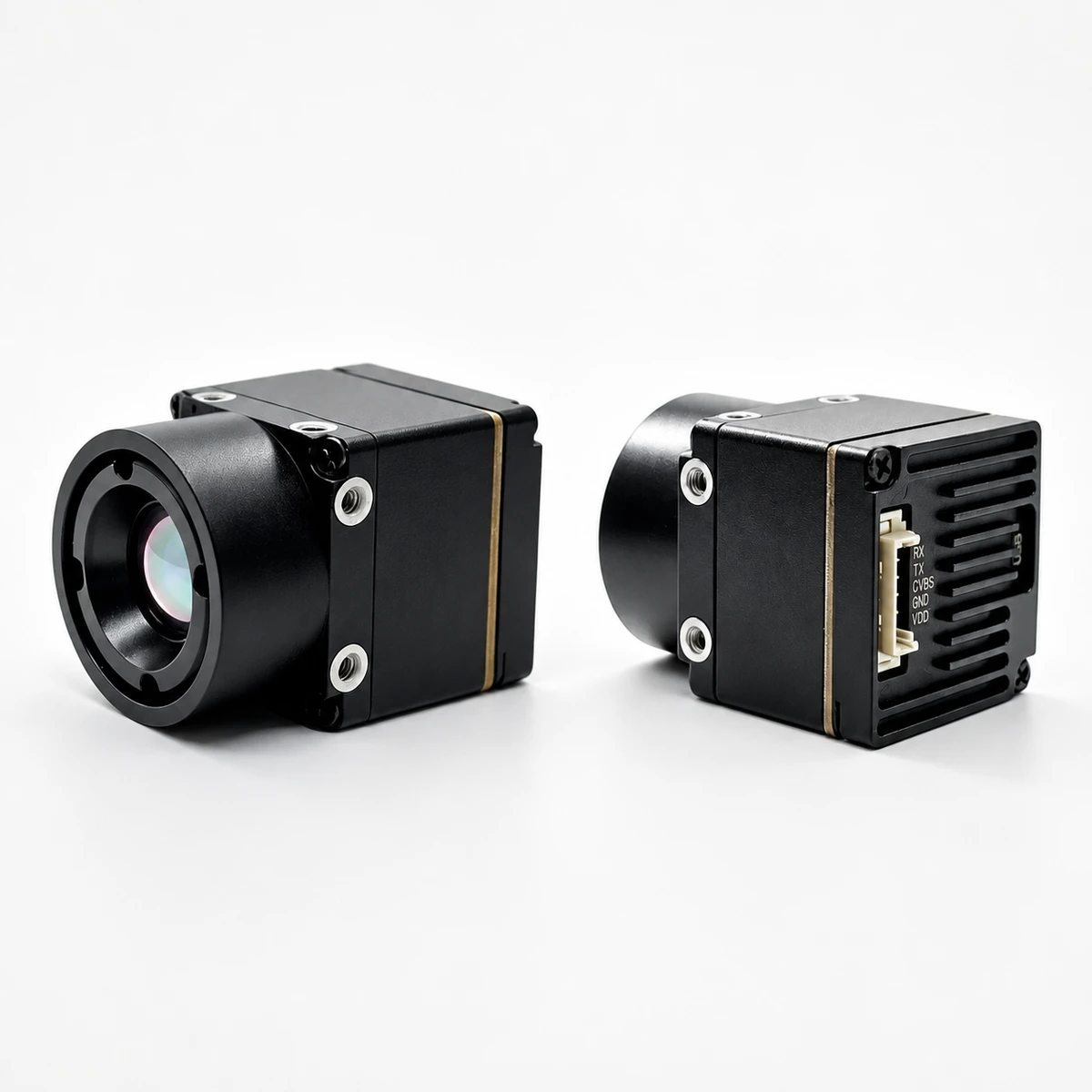
Engineers looking to evaluate different modular form factors and packaging configurations across various sensor tiers can explore our dedicated directory for thermal imaging cores.
Vanadium Oxide (VOx) vs. Amorphous Silicon (a-Si)
The semiconductor material chosen for the microbolometer membrane dictates your baseline signal-to-noise ratio, sensitivity, thermal response time, and operating stability over environmental temperature swings. In the shop, you will primarily encounter two competing detector chemistries:
- ✅ Vanadium Oxide (VOx): VOx is the benchmark detector material for mission-critical industrial, aerospace, and defense applications. It delivers a high Temperature Coefficient of Resistance (TCR), typically running between -2%/K and -3%/K. This elevated TCR gives you exceptional electrical sensitivity to fractional temperature shifts while suppressing 1/f noise. VOx FPAs provide superior spatial uniformity, long-term thermal stability across ambient fluctuations, and fast thermal time constants (typically 8 to 12 ms), making VOx the hands-down choice for dynamic tracking, high-speed drone gimbals, and automated predictive maintenance.
- ⚙️ Amorphous Silicon (a-Si): While a-Si microbolometers leverage standard silicon CMOS fabrication lines to drive down wafer manufacturing costs, they suffer from lower TCR values, higher intrinsic 1/f noise floors, and slower thermal response curves. When deployed on dynamic platforms—like a fixed-wing drone banking hard or an aerial payload climbing rapidly through atmospheric temperature inversions—a-Si sensors suffer from noticeable thermal baseline drift, requiring frequent mechanical shutter recalibrations to clear out spatial fixed-pattern noise (FPN).
Pixel Pitch Transition: 12 µm vs. 17 µm
Modern microbolometer engineering has shifted decisively away from legacy 17 µm and 25 µm processes to standard 12 µm pixel pitch architectures. Moving down to a 12 µm pixel pitch yields major physical and optical advantages for SWaP-constrained designs:
- ✅ Shrunk Optical Format: A 640 x 512 resolution array built on a 17 µm process demands an optical image circle diagonal of roughly 13.9 mm. That exact same 640 x 512 array built on a modern 12 µm node occupies only 7.68 mm x 6.14 mm with a 9.83 mm diagonal. This reduction lets optical engineers cut the physical outer diameter, clear aperture, and mass of expensive Germanium objective lenses by 35% to 50%.
- ✅ Reduced Gimbal Payload Inertia: For airborne pan-tilt gimbals and robotic arms, cutting lens and FPA mass slashes motor torque demands, structural inertia, and continuous electrical draw. This translates directly to extended battery flight endurance and faster, jitter-free tracking response.
Noise Equivalent Temperature Difference (NETD)
Noise Equivalent Temperature Difference (NETD) is the primary figure of merit used to evaluate the thermal sensitivity of an infrared sensor. Expressed in millikelvins (mK), NETD represents the temperature difference at the scene that yields an electrical signal-to-noise ratio (SNR) of exactly one at the sensor readout. Budget commercial thermal sensors run with NETD ratings between 40 mK and 60 mK. Demanding industrial inspection and aerial reconnaissance platforms require high-grade cores rated at ≤30 mK (at F1.0, 25°C). Lower NETD numbers allow a thermal imager camera to cleanly resolve subtle surface temperature gradients across uniform backgrounds—essential for pinpointing sub-surface delaminations, tracking low-contrast living targets hidden within thick foliage, or maintaining visibility in adverse weather like fog, heavy rain, or high humidity where atmospheric moisture suppresses thermal contrast.
2. Optical Selection, IFOV Calculations, and Johnson Criteria
Standard optical glass like N-BK7 or fused silica is completely opaque to infrared light within the 8–14 µm spectral region. Because of this, an LWIR thermal imager camera requires specialized refractive optics ground from monocrystalline Germanium (Ge) or specialized Chalcogenide glass formulations. Germanium offers an exceptionally high refractive index (roughly 4.0 in the LWIR spectrum), which allows optical designers to create fast, compact lenses with wide apertures (typically F1.0 to F1.2) to drive maximum photon flux onto the microbolometer detector plane.
Calculating Instantaneous Field of View (IFOV)
The spatial resolving power of an integrated thermal system is determined by its Instantaneous Field of View (IFOV). IFOV represents the angular field seen by an individual microbolometer pixel projected through the objective lens into object space, calculated in milliradians (mrad):
IFOV (mrad) = [ Pixel Pitch (µm) / Focal Length (mm) ] = p / f
The physical area resolved by a single detector pixel at a given target distance (Range, R) is designated as the Ground Sample Distance (GSD):
GSD = Target Range (m) × IFOV (mrad) × 10⁻³
Let’s run the numbers: a 640 x 512 thermal core built with a 12 µm pixel pitch and fitted with a 9.1 mm lens yields an IFOV of 1.31 mrad. At an operational distance of 100 meters, each individual pixel samples a physical area of 13.1 cm x 13.1 cm. Swap that out for a 35 mm telephoto lens, and the IFOV tightens down to 0.34 mrad. That slashes the GSD at 100 meters down to just 3.4 cm, dramatically increasing your target pixel density for long-range surveillance.
Johnson Criteria for Target Acquisition
Optoelectronic engineers size thermal optics using the established Johnson Criteria. This framework defines the minimum number of resolved spatial line pairs (or pixel cycles) required across the critical dimension of a target (evaluated against a standard human profile of 1.8 m × 0.5 m) to achieve a 50% statistical probability of target acquisition:
- ⚙️ Detection (1.5 line pairs / ~3 pixels): The system operator or edge-AI detector can determine that an object of interest is present in the field of view.
- ⚙️ Recognition (6.0 line pairs / ~12 pixels): The system can classify the target category (e.g., distinguishing a human from a four-legged animal or a passenger car from an SUV).
- ⚙️ Identification (12.0 line pairs / ~24 pixels): The system can discern fine structural details (e.g., identifying carried equipment on personnel or reading distinct vehicle configurations).
The engineering reference matrix below pairs factory Germanium lens options with optical Field of View (FOV), spatial IFOV, and calculated Johnson criteria ranges for a 640 x 512, 12 µm uncooled VOx thermal imager camera:
| Focal Length | Field of View (H × V) | Spatial IFOV | Detection Range (1.8m Human) | Recognition Range | Identification Range |
|---|---|---|---|---|---|
| 4.1 mm | Extra-Wide Angle | Confirmed on RFQ | Order Specific | Order Specific | Order Specific |
| 4.9 mm | 76.2° × 64.2° | 2.45 mrad | 476.0 m | 119.0 m | 60.0 m |
| 9.1 mm | 45.8° × 37.3° | 1.31 mrad | 884.7 m | 221.2 m | 110.6 m |
| 13.0 mm | 33.0° × 26.6° | 0.92 mrad | 1,263.9 m | 316.0 m | 158.0 m |
| 19.0 mm | 22.9° × 18.4° | 0.63 mrad | 1,847.2 m | 461.8 m | 230.9 m |
| 35.0 mm | 12.5° × 10.0° | 0.34 mrad | 3,402.8 m | 850.7 m | 425.4 m |
Engineering Notice: Keep in mind that factory lenses are threaded, focused, and permanently sealed during manufacturing under strict cleanroom conditions. These are not C-mount lenses designed for field swapping. You need to lock down your optical requirements before starting mechanical enclosure design. For a deeper look into optical path design for airborne payloads, check out our guide on high-resolution thermal imaging camera OEM selection.
3. Video Interfaces, Latency, and Power Architecture (MIPI, UVC, CVBS)
Hooking a thermal imager camera into an industrial host processor—whether it is an NVIDIA Jetson Orin, Rockchip RK3588, NXP i.MX8, or an FPGA pipeline—requires matching the physical signaling bus to your compute architecture and system latency budget.
Video Bus Protocol Analysis
Modern thermal camera modules route digital or analog video frames across three main hardware interfaces:
- ⚙️ MIPI CSI-2 (Mobile Industry Processor Interface): MIPI CSI-2 is a high-speed, low-power differential serial bus purpose-built for direct board-to-board links. By streaming raw uncompressed pixel data (such as RAW14 or YUV422) directly into the host processor’s Image Signal Processor (ISP) memory using Direct Memory Access (DMA), MIPI provides the lowest possible latency (typically sub-5 ms). The catch? MIPI trace layouts require strict 100-ohm differential impedance matching, precise trace length matching, and solid shielding when routed over flat flexible cables (FFCs) longer than 150 mm to avoid high-frequency EMI issues.
- ⚙️ USB Video Class (UVC 2.0 / 3.0): The UVC protocol streams video over standard 4-pin USB physical buses (`USB_VDD`, `D-`, `D+`, `GND`). Supported out of the box by Linux (via Video4Linux2 / V4L2), Windows, and ROS2 frameworks, UVC gets rid of the headache of writing custom kernel drivers. The trade-off is higher latency (typically 15 to 30 ms) due to host controller USB bus arbitration, endpoint packetization, and OS frame buffering.
- ⚙️ CVBS (Composite Video Baseband Signal): CVBS provides single-ended analog baseband video (PAL/NTSC reference) over 75-ohm coaxial lines or shielded twisted-pair cabling. While it lacks the high spatial resolution of modern digital links, CVBS remains a top choice in airborne FPV systems and long-range analog video transmitters because of its true real-time streaming (<20 ms glass-to-glass latency) and smooth, predictable degradation under poor RF link conditions without digital frame freezing.
Power Supply Architecture and Rail Filtering
Microbolometer FPAs and Readout ICs are notoriously sensitive to power supply ripple and switching noise. High-frequency noise generated by unshielded DC-DC buck converters or drone Electronic Speed Controllers (ESCs) can bleed directly into the analog bias rails of the FPA, causing horizontal banding artifacts, high temporal noise, and ruined NETD sensitivity.
High-reliability OEM modules feature wide-input voltage tolerance (such as 5–24 V DC or regulated 9–16 V DC). In your system power design, implement a clean two-stage filtering topology:
- ⚙️ Stage 1: Place a common-mode choke and transient voltage suppressor (TVS) diode at the main DC power entry to clamp inductive voltage spikes from battery connections and motor braking.
- ⚙️ Stage 2: Use a dedicated high-PSRR (Power Supply Rejection Ratio) Low-Dropout (LDO) linear regulator right before the thermal core supply pins, backed by high-frequency ceramic decoupling capacitors (100 nF in parallel with 10 µF X7R ceramic caps).
Efficient thermal camera cores maintain a total power draw of <0.7 W, keeping parasitic self-heating low and preserving battery runtime on remote autonomous platforms.
4. OEM Product Hardware Showcase & Technical Comparison
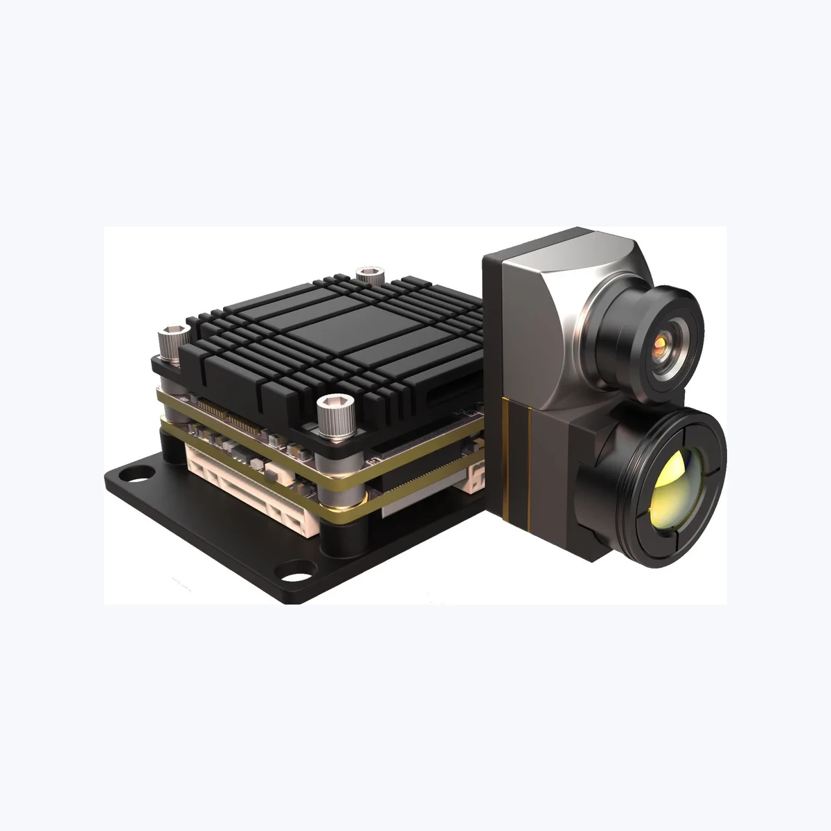
To help you pick the right hardware for your mechanical envelope and compute architecture, let’s look at two production-ready OEM solutions: the ultralight standalone CAMCUDA FlexMini 640 VOx Thermal Module and the TC01-DUAL 4 TOPS Dual-Spectrum UAV AI Tracking Platform.
CAMCUDA FlexMini 640 LWIR Thermal Camera Module
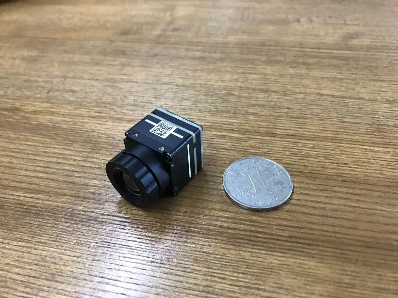
The CAMCUDA FlexMini 640 is an ultralight (23.1 g) OEM thermal imager camera core engineered for direct mechanical and electrical integration into UAV gimbals, handheld monoculars, robotic inspection pods, and compact industrial vision enclosures. It features a 640 x 512 uncooled VOx microbolometer array with a 12 µm pixel pitch, ≤30 mK thermal sensitivity, and 50 Hz native video refresh rates. Operating on a 5–24 V wide-voltage input rail with <0.7 W power draw, it supports CVBS, USB UVC, or MIPI output configurations with an ultra-low reference processing delay of <20 ms.
- Thermal Resolution: 640 x 512 uncooled VOx focal plane array
- Pixel Pitch & NETD: 12 µm pitch, ≤30 mK reference sensitivity (F1.0)
- Frame Rate & Delay: 50 Hz output, <20 ms reference processing latency
- Electrical SWaP: <0.7 W power consumption, 5–24 V DC wide-range input
- Total Module Mass: 23.1 g base architecture
- Lens Stock & Pricing: 9.1 mm ($475.00, In Stock), 4.9 mm ($522.50, In Stock), 4.1 mm ($522.50, In Stock), 13 mm ($522.50, RFQ), 19 mm ($522.50, RFQ), 35 mm ($522.50, RFQ)
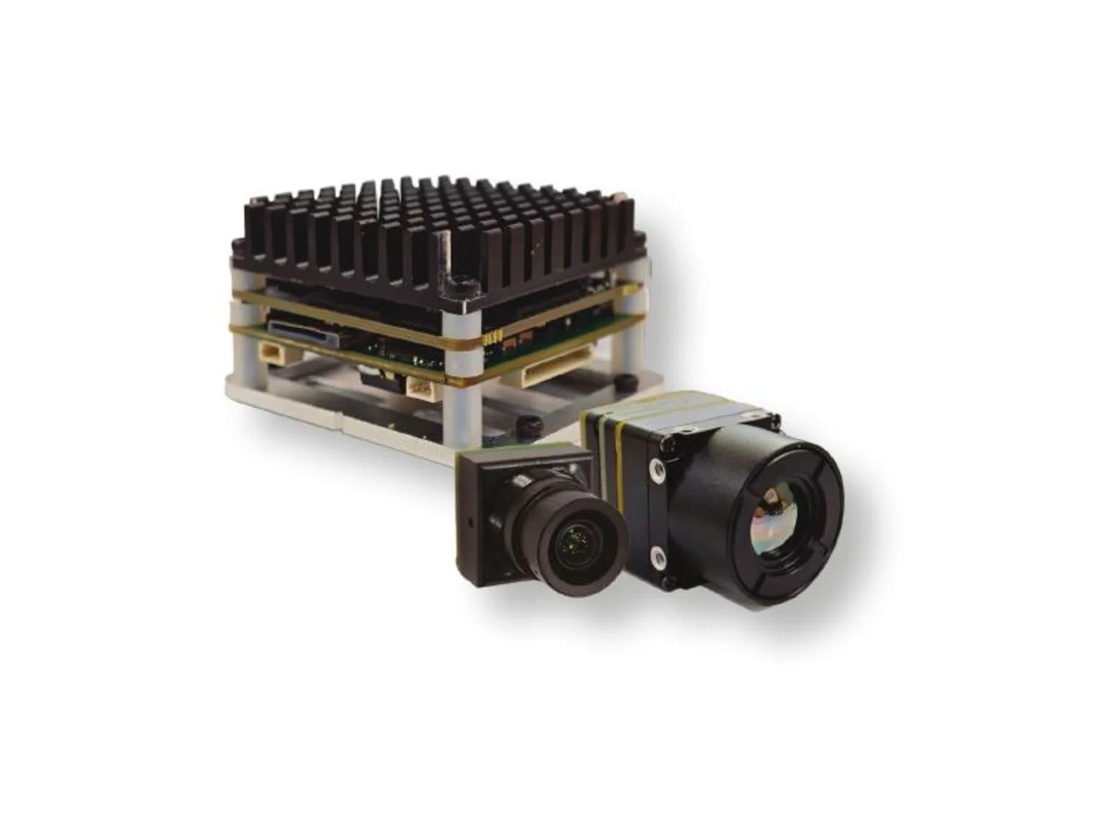
TC01-DUAL 4 TOPS Dual-Spectrum UAV AI Tracking Module
The TC01-DUAL is an edge-AI computing platform combining a 640 x 512 uncooled LWIR thermal channel with a high-resolution 2160 x 1440 60 Hz visible light (EO) camera onto a compact 38 x 38 x 24.5 mm mainboard. Powered by a 4 TOPS neural processing unit, it delivers onboard person and vehicle tracking up to 140 km/h, simultaneous tracking of up to 60 targets, Picture-in-Picture (PIP) display, and dual-light fusion. It connects directly with ArduPilot and BetaFlight flight controllers using the standard CRSF protocol over a 9–16 V DC regulated supply.
- AI Compute Power: 4 TOPS Edge AI neural processing core
- Thermal Channel: 640 x 512 @ 50 Hz, 12 µm pitch, 8–14 µm band, 9.1 mm lens (47.7° H × 38.2° V FOV)
- Visible EO Channel: 1/1.8″ CMOS, 2160 x 1440 @ 60 Hz, 4.37 mm lens (109° H × 57.5° V FOV), 0.001 lux starlight sensitivity
- AI Tracking Specs: Person tracking to 300 m, vehicle tracking to 800 m, 10×10 px minimum target, ≤30 ms latency, speeds up to 140 km/h
- Flight Integration: CRSF protocol support, native BetaFlight and ArduPilot compatibility
- Physical Dimensions: Board: 38 x 38 x 24.5 mm (25.5 x 25.5 mm mounting pattern); Thermal Cam: 29.49 x 19.1 x 19.1 mm; EO Cam: 25.5 x 19.5 x 19.5 mm
Direct Engineering Comparison
The matrix below compares key specifications between the standalone CAMCUDA FlexMini 640 core and the TC01-DUAL AI multi-spectral vision platform:
| Specification Parameter | CAMCUDA FlexMini 640 Standalone Core | TC01-DUAL Thermal Subsystem | TC01-DUAL Visible Subsystem |
|---|---|---|---|
| Sensor Architecture | Uncooled VOx FPA | Uncooled LWIR Microbolometer | 1/1.8-inch CMOS (0.001 lux) |
| Pixel Resolution | 640 × 512 pixels | 640 × 512 pixels | 2160 × 1440 pixels (2K) |
| Frame Rate | 50 Hz | 50 Hz | 60 Hz |
| Pixel Pitch / Aperture | 12 µm / F1.0 | 12 µm / Fast LWIR | 4.37 mm / Wide Angle |
| Focal Length / FOV | 9.1 mm (45.8° × 37.3°) standard | 9.1 mm (47.7° H × 38.2° V) | 4.37 mm (109.0° H × 57.5° V) |
| Processing & AI | Integrated DSP / NUC Engine | 4 TOPS Edge AI NPU (Dual Fusion, PIP, 60 Targets) | |
| Hardware Interfaces | CVBS Analog, USB UVC, or MIPI | USB Host Interface, CRSF Flight Controller Protocol | |
| Supply Voltage | 5–24 V DC Wide-Input | 9–16 V DC Regulated | |
| Physical Dimensions | 23.1 g base architecture | 29.49 × 19.1 × 19.1 mm | 25.5 × 19.5 × 19.5 mm (Board: 38×38×24.5mm) |
For a detailed vendor qualification checklist before locking in PCB designs, consult our thermal camera suppliers OEM RFQ checklist.
5. Dual-Spectrum Sensor Fusion & Edge-AI Tracking Implementation
In autonomous unmanned systems and robotic security pods, relying on a single optical spectrum creates blind spots. High-resolution visible (EO) sensors fail in low-light, dense fog, heavy smoke, or camouflaged conditions. A standalone thermal imager camera provides clear contrast against heat-emitting targets, but it lacks fine structural surface detail—like warning signs, painted markings, and sharp facial features.
Deploying dual-spectrum architectures with onboard edge compute—like the 4 TOPS processing architecture on the TC01-DUAL—solves this problem using multi-sensor spatial registration, real-time pixel fusion, and neural network inference.
Spatial Registration and Parallax Compensation
Because the optical centers of the visible and thermal sensors are separated by a physical baseline distance on the mounting plate, incoming light rays suffer from optical parallax. Before your fusion pipeline can blend the frames, the onboard processor has to apply a dynamic 2D homography transformation:
- ⚙️ Intrinsic & Extrinsic Calibration: During factory calibration, both channels view custom dual-spectrum alignment targets (heated high-contrast checkerboards) to map radial optical distortion and establish precise 3D rotation and translation vectors.
- ⚙️ Field of View Normalization: The wider visible channel (e.g., 109° horizontal) is digitally mapped and cropped to match the narrower field of view of the thermal lens (47.7° horizontal).
- ⚙️ Affine Matrix Warping: Target distance estimates calculated from tracking bounding boxes feed into a real-time affine warping engine, ensuring that thermal heat signatures overlay precisely onto visible edges without double-image ghosting artifacts.
Dual-Light Pixel Fusion and Picture-in-Picture (PIP)
With both image streams spatially locked, the onboard processing core executes real-time fusion pipelines:
- ✅ High-Pass Spatial Edge Blending: The processor runs a high-pass Laplacian filter over the visible luminance (Y) channel to extract crisp structural edges. These high-frequency lines are injected directly into the 8-bit thermal intensity map. This gives you an image that highlights thermal hot spots while preserving readable signage, vehicle outlines, and structural geometry.
- ✅ Picture-in-Picture (PIP) Dynamic Overlay: For situational awareness, the high-resolution visible stream serves as the primary canvas while the thermal channel is displayed as an inset PIP window. Operators or autonomous navigation controllers can reposition or toggle this PIP inset based on AI tracking confidence.
Edge-AI Object Detection & Flight Control Feedback
The onboard 4 TOPS neural processing unit runs lightweight deep learning models (such as INT8-quantized YOLOv8-tiny or MobileNet-SSD) optimized for multi-spectral input tensors. The AI pipeline detects and classifies up to 60 simultaneous targets (persons and vehicles) at speeds up to 140 km/h.
When a target is locked, the edge tracker calculates angular error centroids relative to the optical axis. These tracking error vectors are converted into control commands at 50 Hz and streamed over standard serial protocols (CRSF, MAVLink, or SBUS) directly into BetaFlight or ArduPilot flight controllers. This closes the control loop autonomously, directing gimbal pitch/yaw motors or airframe heading to keep moving targets centered without manual pilot input.
For more insights on integrating industrial optical systems, see Wikipedia – Machine Vision.
6. Thermal Dissipation, Shutter Calibration (NUC), and Mechanical Mounting
Integrating an OEM thermal imager camera into sealed airborne pods, motorized gimbals, or ruggedized industrial enclosures requires strict thermal and mechanical discipline. Uncooled microbolometers measure fractional millikelvin changes across the detector plane; uneven heat build-up inside the housing will distort your readings and degrade image clarity.
Thermal Dissipation & Structural Conduction
The electronics stack in a thermal camera core (ROIC, DSP, FPGA, and power converters) generates localized heat. If that heat bleeds unevenly into the microbolometer detector substrate, it causes spatial non-uniformity and inaccurate thermal readings. Keep these hardware guidelines in mind:
- ⚙️ Direct Conductive Path: Thermally couple the aluminum core housing to your main enclosure using high-conductivity thermal interface materials (TIM), such as gap pads with thermal conductivity $k ge 3.0text{ W/m}cdottext{K}$.
- ⚙️ Component Isolation: Keep high-heat components (like high-power video transmitters, ESC motor drivers, or primary host CPUs) isolated from the thermal core using structural aluminum heatsinks or thermal isolation barriers.
- ⚙️ Germanium Protective Windows: If you are mounting the module inside a sealed, weatherproof housing (IP67/NEMA 4X), the optical window must be monocrystalline Germanium or Chalcogenide glass with an anti-reflective (AR) and Diamond-Like Carbon (DLC) hard coating. Standard acrylic, polycarbonate, or borosilicate glass will completely block LWIR transmission.
Non-Uniformity Correction (NUC) & Solenoid Shutter Operation
Every individual microbolometer pixel has slight differences in responsivity and offset resistance. As the camera’s internal temperature shifts during operation, these differences create spatial fixed-pattern noise (FPN), which shows up as vertical lines or a faint mesh pattern across the video feed.
To eliminate FPN, the core runs a Non-Uniformity Correction (NUC) routine. A miniature electromechanical solenoid drops a uniform-temperature blackbody shutter blade in front of the FPA for 100 to 250 ms. The DSP calculates per-pixel offset coefficients, strips out the spatial noise, and restores an even image baseline.
Integration Strategy for Dynamic Systems: In dynamic drone flight or high-speed tracking, an unexpected shutter calibration will freeze the video stream for a split second, which can break your AI tracking lock. Industrial OEM cores handle this using automated background temperature tracking (only triggering NUC when internal sensor temperatures drift by $Delta T ge 1.0^circtext{C}$), along with a manual UART serial command override (`NUC_TRIGGER`) to block shutter activation during critical tracking runs.
7. Comprehensive Industrial Engineering FAQ
Why do entry-level budget thermal cameras fail in serious industrial and UAV inspection?
Do all LWIR thermal imager cameras provide radiometric temperature output?
How should engineers choose the right focal length and FOV for a fixed thermal module?
How does microbolometer self-heating affect image quality, and how is it mitigated?
What are the primary differences between MIPI CSI-2 and USB UVC for thermal core integration?
📚 References & Further Reading
- Industry Standard: Wikipedia – Thermal Imaging
- Industry Standard: Wikipedia – Machine Vision
- Related Guide: High-Resolution Thermal Imaging Camera OEM Selection Guide
- Related Guide: Thermal Camera Suppliers OEM RFQ Checklist
- Product Catalog: OEM Thermal Imaging Cores & Modules