Cheap Thermal Imaging: OEM Guide to Low-Cost LWIR Modules & Tradeoffs
Cheap Thermal Imaging: OEM Guide to Low-Cost LWIR Modules & Tradeoffs
For systems engineers, robotics architects, and electro-optical payload integrators, the phrase “cheap thermal imaging” has historically felt like a flat-out contradiction. Let’s be honest: Long-Wave Infrared (LWIR) sensing has always battered bills of materials (BOM). You were stuck dealing with low-yield microbolometer fabrication, finicky ceramic hermetic packages, single-point diamond-turned monocrystalline Germanium optics, and specialized signal-processing silicon that cost an arm and a leg. Early attempts to trim these budgets forced teams into painful compromises—slapping low-res 160×120 or 256×192 focal plane arrays onto builds. In the shop, we all know what that looks like: muddy thermal signatures, choked detection ranges, and hardware that falls flat on industrial inspection or autonomous navigation tasks.
Here’s the deal: recent leaps in semiconductor fabrication, sub-12 µm pixel architectures, Wafer-Level Packaging (WLP), and integrated system-on-chip (SoC) signal processing have flipped the economics of uncooled LWIR vision on its head. Sourcing an affordable thermal core doesn’t mean settling for pixelated mud anymore. Production-ready 640×512 Long-Wave Infrared sensor cores now hit price points that make total sense for mass-market commercial builds, field robotics, and unmanned aerial vehicle (UAV) gimbals.
Getting the right balance between unit cost and real-world sensing comes down to understanding the physics and manufacturing tradeoffs under the hood. When picking an OEM thermal engine, you have to weigh pixel pitch scaling, Noise Equivalent Temperature Difference (NETD), radiometric calibration overhead, optical substrates (Germanium vs. Chalcogenide), and your embedded bus options (like MIPI CSI-2, BT.656, and native USB). This engineering breakdown covers the exact mechanics driving thermal imaging costs down, backed by real integration data for dropping high-resolution, low-SWaP (Size, Weight, Power, and Cost) uncooled cores directly into your stack.
Table of Contents
- 👉 1. The Economics of Modern LWIR: What Makes Thermal Imaging “Cheap”?
- 👉 2. Core Engineering Tradeoffs in Low-Cost Thermal Sensors
- 👉 3. Optics and Hardware Interface Optimization for Low-SWaP Builds
- 👉 4. OEM Product Showcase & Benchmarking Cost-Effective 640×512 Cores
- 👉 5. Electrical, Mechanical, and Thermal Dissipation Integration Guide
- 👉 6. Frequently Asked Questions (FAQ)
1. The Economics of Modern LWIR: What Makes Thermal Imaging “Cheap”?
The price drop in uncooled Long-Wave Infrared sensors didn’t happen by accident. It is the direct outcome of disciplined silicon processing, modern packaging, and smarter optical tooling. In the old days, uncooled focal plane arrays (FPAs) built by defense outfits like BAE Systems lived in bulky metal cans or multi-layer ceramic packages. Every single detector die was picked, placed, wire-bonded, baked under a high vacuum with getter materials, and sealed one by one using gold-tin solder preforms. That legacy single-unit pipeline meant high labor costs, painfully long production cycles, and brutal scrap rates whenever a vacuum seal failed on the bench.
Today, high-volume commercial LWIR production runs entirely on Wafer-Level Packaging (WLP). Under WLP, the microbolometer Read-Out Integrated Circuit (ROIC) wafer—holding thousands of active Vanadium Oxide (VOx) sensor arrays—is mated straight to an antireflection-coated silicon or Germanium window wafer etched with microscopic vacuum cavities. These two 8-inch wafers are aligned and bonded under high vacuum using metallic sealing rings. Once joined, the whole sandwich gets diced into finished, vacuum-sealed sensor engines in a single cut. This workflow ramps throughput by orders of magnitude and brings unit packaging costs down to earth.
Another massive factor here is the reduction of bolometer pixel pitch. We’ve marched down from legacy 25 µm and 17 µm nodes straight into 12 µm and 8 µm architectures. In wafer fabrication, the physical die footprint dictates how many operational chips you pull from a single run. Look at the math for a standard 640×512 thermal array:
- ⚙️ Legacy 17 µm FPA: Needs an active sensing footprint of 10.88 mm × 8.70 mm, yielding an optical diagonal of 13.93 mm.
- ⚙️ Modern 12 µm FPA: Tightens the active area down to 7.68 mm × 6.14 mm, cutting the optical diagonal to 9.83 mm.
- ⚙️ State-of-the-Art 8 µm FPA: Packs that same active resolution into just 5.12 mm × 4.09 mm, producing a tiny 6.55 mm optical diagonal.
Because silicon real estate scales quadratically with physical dimensions, an 8 µm 640×512 array takes up less than 25% of the silicon area needed by a 17 µm die at the exact same resolution. That means foundries harvest over four times as many working sensors per 8-inch wafer, instantly lowering raw detector costs.
Shrinking that optical diagonal delivers massive savings on the lens assembly as well. Optical physics dictates that to hit a specific field of view (FOV), the focal length of the objective lens scales directly with the sensor’s diagonal. Shorter focal lengths mean smaller clear optical apertures (Aperture = Focal Length / F-number). An 8 µm or 12 µm core needs far less raw infrared substrate—whether you’re working with monocrystalline Germanium or precision-molded Chalcogenide glass—which knocks down the total module BOM cost.
2. Core Engineering Tradeoffs in Low-Cost Thermal Sensors
When selecting a cost-effective LWIR engine, you have to look past marketing claims and evaluate the hard electro-optical metrics. Cutting corners without checking the numbers can wreck spatial accuracy, sensitivity, and measurement reliability down the line.
2.1 Spatial Resolution vs. Sensor Yield (640×512 vs. 256×192)
Budget thermal devices regularly push low-resolution formats like 120×90, 160×120, or 256×192. These chips are undeniably cheap to manufacture due to massive wafer yields, but their spatial sampling capabilities hit a hard ceiling. In optical payload engineering, spatial resolution is dictated by the Instantaneous Field of View (IFOV):
IFOV (mrad) = [ Pixel Pitch (µm) / Focal Length (mm) ]
Let’s run a practical shop example: an aerial inspection rig operating at a 50-meter standoff distance. A cheap 160×120 sensor with a 12 µm pitch and a 4 mm lens yields an IFOV of 3.0 mrad. At 50 meters out, a single pixel covers a 150 mm square patch on your target. Under standard Johnson criteria for target acquisition, resolving a thermal hot spot—like an overheating 20 mm electrical contact or a fine hairline crack—is mathematically out of reach. The hot anomaly covers only a fraction of the pixel, blending its temperature signature with the surrounding surface and causing significant measurement error.
Step up to an uncooled 640×512 array, and you’re gathering 327,680 discrete thermal points—more than seventeen times the spatial data of that 160×120 sensor. Mated to the right optics, a 640×512 core gives edge vision models, automated flight systems, and thermographers the pixel density they need to spot micro-anomalies at safe standoff distances.
2.2 Thermal Sensitivity (NETD) and Signal-to-Noise Ratio (SNR)
Noise Equivalent Temperature Difference (NETD), specified in milliKelvins (mK), marks the scene temperature difference where the system signal-to-noise ratio hits unity. Simply put: it is the smallest temperature delta your sensor can pull out from its own background electronic noise floor.
Cheap thermal cameras running rough ROIC designs or basic readout electronics often sit at noisy NETD levels of ≥50 mK to 80 mK. Aim those high-noise sensors at uniform scenes—like an open body of water, a flat concrete apron, or building facade insulation—and your feed turns into a muddy, low-contrast image loaded with temporal grain. High-grade uncooled VOx cores pull that sensitivity down to ≤30 mK to ≤40 mK at F1.0, preserving clean object edges and contrast across low-delta scenes.
2.3 Qualitative Imaging vs. Calibrated Radiometry
A significant cost driver in OEM thermal engines comes down to whether you need relative imaging or absolute temperature calibration:
- ✅ Qualitative Thermal Modules: Purpose-built for situational vision and target spotting. These cores run on-board Automatic Gain Control (AGC), histogram balancing, and dynamic contrast stretching to turn raw 14-bit bolometer data into standard 8-bit visual streams (White Hot, Black Hot, Rainbow). Because individual pixel brightness shifts relative to what is in the frame, they don’t give you absolute temperature values. Skipping the factory calibration process keeps these engines budget-friendly for FPV piloting, industrial navigation, and security sweeps.
- ✅ Radiometric Thermal Modules: Packed with per-pixel factory calibration lookup tables (LUTs) that translate raw microbolometer resistance swings directly into calibrated temperature readouts (°C, °F, or Kelvin). Getting this right requires running every module through multi-point temperature chambers with blackbody sources over wide ambient ranges (-40°C to +80°C), paired with real-time housing compensation algorithms. Radiometric modules are non-negotiable for substation monitoring, flare-stack checks, and fire prevention. For deeper insights on industrial calibration architectures, review our breakdown on uncooled LWIR thermal modules for outdoor security and industrial monitoring.
2.4 Frame Rate Architecture: 9 Hz vs. 30 Hz / 50 Hz / 60 Hz
Export controls (including US ITAR/EAR and global dual-use rules) restrict standard consumer thermal imagers to refresh rates below 9 Hz. While 9 Hz works for a static handheld tool, that 111 ms per-frame latency causes visible stutter and smearing on any moving platform.
For robotic control loops, drone gimbals, and automated factory lines, high frame rates are critical. Industrial OEM cores operate at 30 Hz, 50 Hz, or 60 Hz. A 60 Hz output cuts frame latency down to ~16.6 ms, delivering the temporal response needed for tight control loops, stable FPV tracking, and artifact-free captures of moving targets.
3. Optics and Hardware Interface Optimization for Low-SWaP Builds
Building a solid low-cost thermal payload requires matching the optical train and the electrical bus directly to your host platform.
3.1 Chalcogenide vs. Germanium Optics
Infrared glass makes up a big slice of any LWIR module’s total cost. Standard optical glasses like BK7 or fused silica block the 8–14 µm spectrum completely, forcing us to use specialized IR-transmissive substrates:
- ⚙️ Monocrystalline Germanium (Ge): Features a high refractive index ($n \approx 4.0$), allowing thin optical elements with shallow curves and minimal aberration. But Germanium is heavy, expensive, and requires Single-Point Diamond Turning (SPDT). It is also prone to thermal runaway: as ambient heat rises, internal carrier absorption climbs, and the lens elements can turn opaque at higher operating temps.
- ⚙️ Chalcogenide Glass: Chalcogenide blends (such as $Ge_{28}Sb_{12}Se_{60}$ or $As_{40}Se_{60}$) can be hot-pressed into precision aspheric-diffractive elements in volume batches. Precision molding bypasses the diamond-turning machine entirely, slashing production costs for OEM runs. Chalcogenide also exhibits a much lower change in refractive index across temperature ($dn/dT$), enabling stable passive athermalization across wide operational envelopes (-40°C to +80°C) without motorized focus hardware.
3.2 Digital Video and Embedded Bus Integration (MIPI, BT.656, USB)
Plugging an uncooled core into modern edge processors (NVIDIA Jetson, Raspberry Pi Compute Module, NXP i.MX8, or Rockchip RK3588) requires native hardware compatibility. Choosing a core with the right output bus saves board space, BOM cost, and pipeline latency by dropping external bridge chips:
- ⚙️ 2-Lane MIPI CSI-2: Feeds raw pixel data straight into the host processor’s hardware Image Signal Processor (ISP), bypassing capture cards and keeping glass-to-glass latency down to milliseconds.
- ⚙️ BT.656 / 8-bit LVCMOS: A standard, rock-solid parallel interface that hooks cleanly into microcontrollers, hardware video encoders, and digital radio links.
- ⚙️ Native USB 2.0 (UVC Class): Delivers driver-free streaming into Linux (V4L2), Windows, or ROS environments for fast software prototyping and test-bench setups.
- ⚙️ Analog CVBS (PAL / NTSC): Provides a direct, zero-latency composite feed for analog 5.8 GHz FPV transmitters, vehicle monitors, and legacy displays via simple external line buffering.
To evaluate mechanical envelopes, lens focal lengths, and bus layouts, check out our full CAMCUDA product catalog, and compare specs against industry benchmarks like Teledyne FLIR.
4. OEM Product Showcase & Benchmarking Cost-Effective 640×512 Cores
Here is an engineering overview of two high-performance, cost-effective 640×512 LWIR cores designed specifically for SWaP-constrained industrial, drone, and field robotics applications.
CAMCUDA AeroMini 640×512 Uncooled LWIR USB Thermal Camera Core
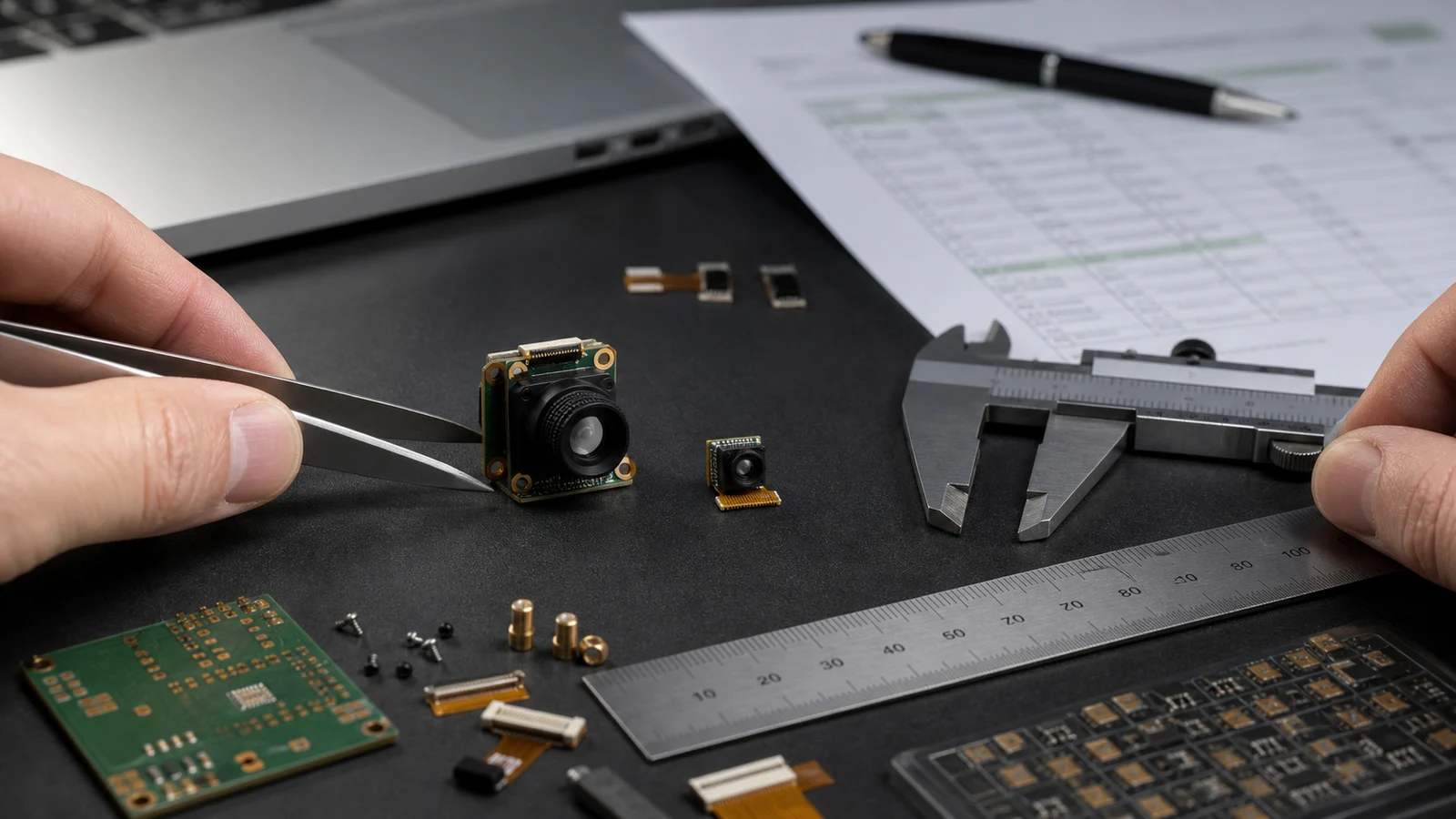
The CAMCUDA AeroMini 640 pairs a 640×512 uncooled Vanadium Oxide (VOx) focal plane array with a 12 µm pixel pitch in a robust, compact housing built for drone payloads, industrial UAV gimbals, and mobile rovers. Weighing under 20 grams (bare core) with dimensions of 21 × 21 × 28 mm, the AeroMini 640 balances ultra-low SWaP with high sensitivity (≤30 mK at F1.0). The module is factory-built in standard 60 Hz or optional 30 Hz configs for high-speed situational awareness, alongside a dedicated 25 Hz radiometric model for precision thermography.
Key Technical Specifications
| Parameter | Specification | Configuration Notes |
|---|---|---|
| Resolution | 640 × 512 pixels | Both versions |
| Detector Type | VOx Uncooled FPA | Long-Wave Infrared |
| Pixel Pitch | 12 µm | Both versions |
| Spectral Response | 8–14 µm | LWIR Atmospheric Window |
| NETD Sensitivity | ≤30 mK @ 25°C, F1.0 | High-contrast thermal acuity |
| Frame Rates | 60 Hz default / 30 Hz option / 25 Hz Radiometric | Factory configured |
| Power Consumption | <0.5 W (typical @ 25°C) | Core module typical |
| Supply Voltage | 5 V or 12 V (board dependent) | POWER_IN pins are 5V inputs |
| Digital Video Output | YUV, USB, BT.656 | Board and firmware dependent |
| Analog Video & Control | CVBS (PAL/NTSC); UART, RS232, RS422 | Serial communication dependent on board |
| Core SWaP Envelope | 21 × 21 × 28 mm; <20 g | Excludes lens and mounting flange |
| Temperature Range | -20°C to +550°C (Radiometric version) | Enquiry only |
| Operating Temp Range | -40°C to +80°C | Storage: -50°C to +85°C |
AeroMini 640 Lens Options & Field of View
| Lens Focal Length | Horizontal × Vertical FOV | Camera Version Compatibility |
|---|---|---|
| 4 mm | 100° × 82° | Non-radiometric |
| 7 mm | 64° × 52° | Non-radiometric |
| 9 mm | 48.7° × 38.6° | Non-radiometric • Radiometric enquiry |
| 13 mm | 31.9° × 25.7° | Non-radiometric • Radiometric enquiry |
| 15 mm | 29.3° × 23.5° | Enquiry version |
| 18 mm | 24.2° × 19.5° | Non-radiometric • Radiometric enquiry |
| 25 mm | 17.5° × 14° | Non-radiometric |
| 35 mm | 12.5° × 10° | Non-radiometric |
| 50 mm | 8.8° × 7° | Non-radiometric |
| 60 mm | 7.3° × 5.8° | Non-radiometric |
CAMCUDA SuperMini 640 / 640T Ultra-Light LWIR Thermal Camera Module
The CAMCUDA SuperMini 640 / 640T uses an advanced 8 µm pixel pitch to fit full 640×512 imaging into a tiny 13 × 13 × 13.4 mm core footprint weighing just 3.5 grams. Engineered for weight-critical UAVs, tight micro-gimbals, and wearable diagnostic gear, it pulls under 0.5 W in typical operation. The series comes in two application-specific builds:
- ✅ CAMCUDA SuperMini 640 (Imaging Only): Runs at 50 Hz with 8-bit LVCMOS/BT656 and 2-lane MIPI outputs for responsive low-latency piloting and vision pipelines.
- ✅ CAMCUDA SuperMini 640T (Thermographic): Runs at 30 Hz with CDS3 and MIPI telemetry paths, outputting calibrated temperature streams across dual ranges (-20°C to +150°C and 100°C to +650°C).
Electrical Interface & Power Rail Requirements
The SuperMini core exposes its signals via a Hirose DF40C-30DP-0.4V(51) 30-pin header. Clean, low-noise power rails are essential to protect the sensor’s ≤40 mK sensitivity:
| Signal / Power Path | Voltage & Tolerance Requirement | Integration & Noise Constraints |
|---|---|---|
| MAIN_POWER | 3.8–5.2 V (Typical 5.0 V) | 10 mV p-p maximum allowable noise |
| +3.3 V Rail | 3.28–3.32 V | 10 mV p-p maximum ripple |
| +1.8 V Rail | 1.78–1.82 V | 1 mV RMS maximum noise (1 Hz–50 kHz) |
| Digital Video | 8-bit LVCMOS / 2-lane MIPI CSI-2 | 640: BT656 • 640T: CDS3 format |
| Control Interface | UART (1.8 V logic levels) | TX/RX defined from core perspective |
| USB / CVBS | USB 2.0 D+/D- pins; CVBS pin | CVBS output requires external video-buffer IC |
Athermalized Lens Configurations (F1.0)
| Lens Focal Length | Horizontal × Vertical FOV | IFOV Resolution | Optical Type |
|---|---|---|---|
| 3.7 mm | 90.0° × 68.2° | 2.16 mrad | F1.0 Athermalized Wide Angle |
| 6.1 mm | 46.6° × 37.6° | 1.31 mrad | F1.0 Athermalized Wide Field |
| 8.7 mm | 40.0° × 32.2° | 0.92 mrad | F1.0 Athermalized Standard |
| 11 mm | 24.9° × 20.0° | 0.73 mrad | F1.0 Athermalized Narrow Field |
Architecture Comparison: AeroMini 640 vs. SuperMini 640
| Engineering Parameter | CAMCUDA AeroMini 640 | CAMCUDA SuperMini 640 / 640T |
|---|---|---|
| Active Sensor Resolution | 640 × 512 pixels | 640 × 512 pixels |
| Bolometer Pixel Pitch | 12 µm | 8 µm |
| Thermal Sensitivity (NETD) | ≤30 mK @ 25°C, F1.0 | ≤40 mK @ 25°C, F1.0 |
| Core Dimensions (Excl. Lens) | 21 × 21 × 28 mm | 13 × 13 × 13.4 mm |
| Core Weight (Excl. Lens) | <20 g | <3.5 g |
| Typical Power Draw (@ 25°C) | <0.5 W | ≤0.5 W |
| Frame Rate Options | 60 Hz default / 30 Hz option / 25 Hz Radiometric | 50 Hz (SuperMini 640) / 30 Hz (SuperMini 640T) |
| Primary Video Interfaces | YUV, USB 2.0, BT.656 | 2-lane MIPI CSI-2, 8-bit LVCMOS / BT656, USB 2.0 |
| Analog & Control I/O | CVBS (PAL/NTSC); UART, RS232, RS422 | CVBS (requires external buffer); UART (1.8 V logic) |
| Athermal Lens Options | 4 mm to 60 mm (10 lens models) | 3.7 mm, 6.1 mm, 8.7 mm, 11 mm |
| Operating Temperature | -40°C to +80°C | -40°C to +80°C |
5. Electrical, Mechanical, and Thermal Dissipation Integration Guide
Dropping an uncooled 640×512 microbolometer core into a custom enclosure demands attention to power conditioning and thermal management. Here is how to keep sensor noise low and avoid calibration drift on the bench:
1. Power Supply Conditioning & Ripple Management: An uncooled microbolometer detects incoming thermal radiation by measuring micro-resistance changes across suspended Vanadium Oxide bridges. We are talking about microvolt-level signal variations inside the ROIC. If your DC feed carries switching noise from high-frequency DC-DC buck converters, that noise will bleed straight into the integration capacitors. When designing power circuits for sensitive engines like the CAMCUDA SuperMini series, keep the +1.8V analog rail below 1 mV RMS (1 Hz–50 kHz), and cap the MAIN_POWER rail at 10 mV p-p ripple. Place dedicated, low-noise low-dropout (LDO) linear regulators with high PSRR right next to the camera header.
2. Thermal Dissipation & Gradient Control: Thermal detectors react to raw heat transfer, which means uneven casing temperatures will distort scene readings. Localized heat sources—such as high-power SoCs, motor drivers, or RF transmitters—must not dump uneven thermal gradients across the sensor housing. Ensure the core is tied to a heat sink or chassis conduction path that moves heat away uniformly, keeping thermal gradients across the array plane to a minimum.
3. Non-Uniformity Correction (NUC) Shutter Calibration: All uncooled VOx focal plane arrays drift as ambient operating temperatures swing. To keep the image uniform, the core periodically drops an internal mechanical shutter for a single-point Non-Uniformity Correction (NUC) cycle to re-zero pixel offsets. For robotic vision or UAV flights, shutter events should be triggered over software commands. You can track vehicle dynamics over UART, pausing automatic NUC sweeps during high-G turns or fast descent passes, and firing the calibration routine only when the craft is level and stable.
For more integration reference circuits and driver walkthroughs, check out the resources on the CAMCUDA technical blog.
6. Frequently Asked Questions (FAQ)
Why do sub-$400 consumer thermal cameras often fail for industrial or drone inspection?
What is the technical difference between qualitative thermal vision and radiometric temperature measurement?
How can OEM engineers achieve cost-effective thermal integration without sacrificing 640×512 resolution?
📚 References & Further Reading
- Industry Standard: Explore commercial thermal systems and detector benchmarks from Teledyne FLIR.
- Defense & Aerospace Standards: Review microbolometer and electro-optical payload developments at BAE Systems.
- Related Technical Guide: Read our technical guide on uncooled LWIR thermal modules for outdoor security and industrial monitoring.
- OEM Solutions Catalog: Browse available LWIR cores and sensor configurations in the CAMCUDA product catalog.
- Engineering Knowledge Base: Access integration notes, whitepapers, and SDK documentation on the CAMCUDA technical blog.