Thermal Imaging Guide: LWIR Sensor Selection, Radiometry, and OEM Integration
Thermal Imaging Guide: LWIR Sensor Selection, Radiometry, and OEM Integration
Thermal imaging has completely broken out of its traditional military niche. Today, it’s a frontline sensing modality across autonomous mobile robots, commercial unmanned aerial systems (UAS), industrial machine vision, optical gas detection, and predictive maintenance rigs. But here’s the deal: dropping an uncooled Long-Wave Infrared (LWIR) sensor core into a custom OEM embedded platform is anything but plug-and-play. You’re balancing a messy matrix of optoelectronic trade-offs where every single engineering decision ripples across your power budget, mechanical envelope, and thermal equilibrium.
If you’re an embedded hardware engineer or system architect, you know the headache. You have to juggle focal plane array (FPA) semiconductor chemistry, pixel pitch reduction vs. diffraction limits, mechanical shutter calibration cycles, raw radiometric temperature math, and brutal Size, Weight, Power, and Cost (SWaP-C) constraints. Squeeze the pixel pitch down to shave optical mass, and your optical assembly suddenly runs headfirst into LWIR diffraction limits. Cut down on power filtering to save board space, and your digital switching noise bleeds right into your analog readout circuit, wrecking your noise floor.
Whether you’re building a lightweight commercial micro-gimbal or swapping out legacy analog camera pipelines in an industrial processing plant, the thermal core you pick dictates your optical efficiency, signal-to-noise ratio (SNR), processor load, and effective detection range. In this guide, we’ll get into the weeds: the solid-state physics of uncooled microbolometers, radiometric math versus visual-only dynamic range compression, electrical power routing and thermal sinking best practices, and side-by-side performance benchmarks for high-framerate OEM thermal engines.
Table of Contents
- 👉 1. Physics of Thermal Imaging: Atmospheric Windows and LWIR Detectors
- 👉 2. Microbolometer Architecture: VOx, Pixel Pitch (12 µm vs. 8 µm), and NETD
- 👉 3. LWIR Optics: IFOV, Athermalization, and Johnson’s Criteria
- 👉 4. Radiometric Calibration vs. Standard Imaging Pipelines
- 👉 5. OEM Electrical, Thermal, and Interface Integration
- 👉 6. Drone and Gimbal Payload Engineering
- 👉 7. OEM Module Technical Specifications: AeroMini 640 vs. SuperMini Series
- 👉 8. Frequently Asked Technical Questions
1. Physics of Thermal Imaging: Atmospheric Windows and LWIR Detectors
To spec thermal hardware properly, you need to throw out standard visible-light assumptions. Visible and near-infrared (NIR) cameras commonly image reflected illumination using photon-sensitive detectors. Thermal sensors, by contrast, measure raw electromagnetic radiation emitted directly by matter as a function of its surface temperature and emissivity. Everything in the universe above absolute zero (0 Kelvin / -273.15°C) emits radiation across a continuous spectrum, governed by Planck’s Radiation Law.
When you integrate Planck’s spectral distribution curve across all wavelengths, you arrive at the Stefan-Boltzmann Law, which describes total radiant exitance (emitted power per unit area):
W = ε σ T4
Where W is total radiant exitance (Watts per square meter), ε is the total hemispherical emissivity at temperature T, ranging from 0 for an ideal perfect reflector to 1.0 for an ideal blackbody, σ is the Stefan-Boltzmann constant (5.670374 × 10⁻⁸ W·m-2·K-4), and T is thermodynamic temperature in Kelvin. Notice that temperature is raised to the fourth power. The resulting image contrast also depends on emissivity, background radiation, optics, and detector noise.
Now, pair that with Wien’s Displacement Law, which proves that the peak emission wavelength shifts shorter as an object gets hotter. For real-world terrestrial targets—humans, vehicles, industrial machinery, and soil operating around ambient temperatures (~300 K / 27°C)—the peak radiation curve lands squarely at approximately 9.6 μm. That places terrestrial heat signatures right inside the 8.0 to 14.0 μm Long-Wave Infrared band.
Earth’s atmosphere isn’t an open pipe for infrared radiation. Molecular resonance from atmospheric water vapor (H2O), carbon dioxide (CO2), and ozone (O3) creates broad absorption bands that block most infrared light over distance. Optical engineers design systems around two distinct operational transmission windows:
- ⚙️ Mid-Wave Infrared (MWIR, 3.0 to 5.0 μm): Ambient-temperature targets emit less radiation in MWIR than in LWIR. Relative atmospheric attenuation depends on humidity, aerosols, weather, and path length. Many high-performance MWIR cameras use cooled photon detectors, such as InSb or MCT. Detector operating temperature, cooldown time, power, size, and cooler service life depend on the specific design; modern high-operating-temperature detectors can reduce cooling requirements.
- ⚙️ Long-Wave Infrared (LWIR, 8.0 to 14.0 μm): Directly overlays the peak emission curve for everyday ambient-temperature targets. Many compact LWIR engines use uncooled microbolometer arrays. These avoid mechanical cryo-coolers and can suit small payloads, but startup time, power consumption, and shutter operation depend on the selected module.
If you’re architecting systems for border surveillance, tactical observation, or search-and-rescue, integrating proven cores from specialized thermal observation devices can provide passive day-and-night imaging without active illumination and improve visibility through some smoke, dust, or light fog. Dense foliage and adverse atmospheric conditions can still obscure targets.
2. Microbolometer Architecture: VOx, Pixel Pitch (12 µm vs. 8 µm), and NETD
Look inside an uncooled LWIR camera engine and you won’t find traditional semiconductor photodiodes. In a microbolometer focal plane array, each individual pixel is a micromechanical thermal bridge: an ultra-thin radiation-absorbing membrane suspended a few microns above a silicon Readout Integrated Circuit (ROIC). The membrane is supported by micro-machined silicon nitride legs that act as high thermal-resistance pathways.
When incoming LWIR energy hits the membrane, the membrane heats up. That micro-temperature shift changes the electrical resistance of the thin film deposited on the bridge. The ROIC underneath measures this resistance shift across every pixel in the matrix by firing a precision bias voltage or current pulse, translating thermal flux into discrete analog voltage levels before pushing them into the onboard analog-to-digital converters (ADCs).
Vanadium Oxide (VOx) vs. Amorphous Silicon (a-Si)
In the shop, the sensing material, membrane structure, and readout design together influence sensitivity and signal stability:
- ✅ Vanadium Oxide (VOx): VOx is widely used in high-performance OEM modules. VOx films can exhibit a Temperature Coefficient of Resistance (TCR) of approximately -2% to -3% per Kelvin; TCR and 1/f (flicker) noise depend on film fabrication. Sensitivity and thermal response also depend on pixel construction and readout design; verify measured NETD and motion response for the selected array.
- ⚙️ Amorphous Silicon (a-Si): a-Si benefits from established silicon fabrication processes and is also used in high-performance thermal imagers. TCR, noise, sensitivity, and thermal response depend on the material process, pixel structure, and readout electronics; a-Si does not necessarily imply a slower or less sensitive camera.
Pixel Pitch Scaling: The Shift from 17 μm and 12 μm to Sub-Miniature 8 μm
Pixel pitch—the physical center-to-center distance between neighboring detector pixels—is the single most critical lever in modern thermal camera packaging. Over the last decade, the industry moved from 25 μm down to 17 μm, standardized on 12 μm, and has now pushed into sub-miniature 8 μm nodes.
Here’s why 8 μm technology is a game-changer for payload engineering: a 640 × 512 array built on an 8 μm pitch occupies an active diagonal of just ~6.55 mm, compared to ~9.83 mm for a 12 μm array. That roughly 55% reduction in focal plane area means you can shorten your lens focal length by roughly 33% to maintain the exact same Field of View (FOV). Shorter focal lengths mean smaller clear optical apertures at equivalent F-numbers, which can reduce the volume, outer diameter, and mass of Germanium elements. This supports compact optical designs, but the SuperMini figure of under 3.5 grams is for the bare core, excluding optics and expansion boards.
However, physics imposes strict constraints at 8 μm. Because 8 μm is right on par with the 8–14 μm wavelengths being detected, the optical system hits the diffraction limit fast. The diffraction-limited Airy disk diameter is approximately d = 2.44 × λ × F-number. At a 10 μm wavelength, even F1.0 gives a diameter of about 24.4 μm, larger than an 8 μm pixel. Faster optics can improve diffraction-limited MTF and throughput, but F1.0 is not a universal requirement; evaluate the complete lens-and-detector MTF and sensitivity.
Noise Equivalent Temperature Difference (NETD)
Noise Equivalent Temperature Difference (NETD) is the primary metric for microbolometer sensitivity. It represents the smallest temperature change in a scene that generates an electrical signal equal to the sensor’s internal electronic noise floor (SNR = 1). NETD is measured in millikelvins (mK):
Example specification: NETD ≤ 40 mK @ 25°C, F1.0
A lower NETD can help reveal small surface-temperature contrasts under the specified test conditions. Detecting moisture-related surface patterns, solar-cell defects, bearing heating, or people also depends on target size, optics, contrast, atmosphere, and the application; a NETD rating alone does not guarantee detection or visibility through drywall.
3. LWIR Optics: IFOV, Athermalization, and Johnson’s Criteria
You cannot use standard visible-light optical glass (such as N-BK7 or fused silica) for thermal imaging. Ordinary visible-light glass is unsuitable for transmission optics across the 8–14 μm band. LWIR optical assemblies commonly use specialized crystalline and chalcogenide materials:
- ⚙️ Monocrystalline Germanium (Ge): The workhorse of thermal optics. Germanium provides a very high refractive index (n ≈ 4.00 at 10 μm), which allows strong optical power with relatively shallow surface curvature; spherical aberration still depends on lens shape and the complete optical design. But Germanium has a massive thermal refractive index drift (dn/dT ≈ 3.96 × 10⁻⁴ / °C at 10 μm). Without optical compensation, ambient temperature shifts will throw the image out of focus. Furthermore, Germanium transmission decreases at elevated temperatures as free-carrier absorption increases; verify the optical supplier’s temperature limit rather than treating +100°C as a universal opacity threshold.
- ⚙️ Chalcogenide Glass (e.g., GASIR, BD6): Moldable amorphous glasses containing one or more chalcogen elements, such as selenium, sulfur, or tellurium, combined with other elements. Common optical grades such as GASIR and BD6 have a much lower dn/dT than Germanium and can be precision-pressed into aspheric and diffractive geometries. They are ideal for hybrid optical stacks designed to hold focus across wide thermal swings.
Passive Optical Athermalization
Thermal modules mounted on industrial assets or aircraft routinely experience ambient swings from -20°C up to +60°C. If your optical stack isn’t athermalized, focus drifts rapidly. Passive mechanical and optical athermalization pairs specific lens elements (Germanium + Chalcogenide) with precision-machined mechanical housing barrels (using aluminum, invar, or engineered polymers). The thermal expansion of the barrel physically offsets the refractive index shift of the glass, maintaining high MTF without the added mass, cost, and power draw of motorized focus motors.
Instantaneous Field of View (IFOV) and Spatial Resolution
Instantaneous Field of View (IFOV) is the spatial angle covered by a single pixel in the array. It dictates your spatial resolution at a given distance:
IFOV = Pixel Pitch (p) / Focal Length (f) [radians]
Multiply IFOV in radians by range in meters to estimate the projected pixel footprint in meters; if IFOV is in milliradians, divide the product by 1,000. For instance, a 12 μm sensor behind a 9 mm lens yields an IFOV of 1.33 mrad, projecting a 1.33-meter sampling spot at 1,000 meters. Meanwhile, an 8 μm sensor with an 11 mm lens delivers an IFOV of 0.73 mrad, resolving a much tighter 0.73-meter spot at that same 1,000-meter range.
Johnson’s Criteria and Illustrative Sampling
Johnson’s Criteria relate resolved target detail to acquisition probability under stated conditions. The table below instead uses illustrative assumptions of 3, 12, and 24 pixels across a selected target dimension, equivalent to 1.5, 6, and 12 pixel pairs. These are not universal Johnson thresholds or verified detection ranges:
| Illustrative Task | Line-Pair Equivalent | Assumed Pixels on Target | Operational Meaning |
|---|---|---|---|
| Detection | 1.5 line pairs | ≈ 3 pixels | An object or hot spot is present in the scene. |
| Recognition | 6.0 line pairs | ≈ 12 pixels | The class of target is discernable (e.g., human vs. car vs. deer). |
| Identification | 12.0 line pairs | ≈ 24 pixels | Distinguishing a more specific target type (e.g., pickup truck vs. armored vehicle). |
When designing integrated security payloads that require multi-sensor tracking, engineers often cross-reference LWIR video with multi-spectral hardware from specialized field observation devices to ensure accurate target correlation in diverse field conditions.
4. Radiometric Calibration vs. Standard Imaging Pipelines
One of the most common architectural mistakes is treating an imaging-only thermal core as a radiometric (thermographic) core. While both use uncooled microbolometers, their digital signal processing (DSP) pipelines and output data structures are built for entirely different jobs.
Imaging-Only Core Architecture
Imaging-only cores are tuned purely for visual contrast and edge clarity. The goal is to maximize image dynamic range for human eyes or downstream edge-AI computer vision algorithms:
- ⚙️ Non-Uniformity Correction (NUC): Normalizes gain and offset differences across all microbolometer pixels.
- ⚙️ Defective Pixel Concealment: Flags dead or noisy pixels and interpolates them in real time using clean neighboring pixels.
- ⚙️ Dynamic Range Compression: The ADC precision and available output formats depend on the core. Automatic gain control and contrast enhancement can map higher-bit-depth image data to an 8-bit display stream (256 grayscale levels); this processing does not preserve all radiometric information.
- ⚙️ Palette Mapping: Maps display values to supported grayscale or pseudo-color palettes and sends video through the selected interface. Palette support depends on the output mode; for example, SuperMini LVCMOS does not support pseudocolor.
Radiometric / Thermographic Core Architecture
Radiometric cores provide calibrated data for estimating surface temperature within their specified measurement ranges and accuracy conditions, rather than only a high-contrast display image:
- ⚙️ Multi-Point Blackbody Factory Calibration: Radiometric factory calibration relates measured infrared signals to known blackbody reference temperatures. Calibration coverage and stored correction data are model-specific.
- ⚙️ Real-Time Parametric Radiance Compensation: Accurate surface-temperature estimates require accounting for emissivity, reflected radiation, and the measurement path. Available compensation settings and whether processing occurs in the module or host depend on the selected model.
- ⚙️ Raw Radiometric Digital Output: Radiometric data must be decoded using the selected model and output mode. CAMCUDA SuperMini 640T supports image and temperature data through CDS3 and MIPI; follow its documented packet format and mode-specific temperature conversion rather than assuming a generic Kelvin-per-count scale. Temperature-data rules do not apply to imaging-only CAMCUDA SuperMini 640.
Choose a radiometric module when the application requires calibrated temperature values or temperature-based thresholds. Imaging-only modules can support qualitative heat-pattern observation, but do not provide those measurements.
5. OEM Electrical, Thermal, and Interface Integration
When you’re routing an uncooled microbolometer into a host PCB, you are working with an ultra-sensitive analog circuit. Microbolometers detect small resistance changes caused by absorbed infrared radiation. Supply noise can degrade image quality, so verify each rail at the module connector against its published limits.
Power Rail Design and Noise Mitigation
- ⚙️ Analog Rail Cleanliness: For the CAMCUDA SuperMini 640 / 640T bare core, the +1.8 V input must remain within 1.78–1.82 V with maximum noise of 1 mV RMS over 1 Hz–50 kHz. Choose regulation and decoupling to meet the module specification at the connector.
- ⚙️ Main Power Rail Ripple: CAMCUDA SuperMini 640 / 640T requires MAIN_POWER at 3.8–5.2 V and a separate +3.3 V input at 3.28–3.32 V, each with maximum noise of 10 mV p-p, plus the +1.8 V rail. AeroMini power input depends on the board; its illustrated POWER_IN1 / POWER_IN2 pins are 5 V inputs and must not be connected to 12 V.
- ⚙️ Decoupling Layout: Place local decoupling close to the relevant power and ground connections. Select capacitance, regulator stability, and layout for the approved module and interface board, and verify noise at the connector.
Electrical Interface Standards
- ⚙️ Hirose 30-Pin Board-to-Board (e.g., DF40C-30DP-0.4V): The CAMCUDA SuperMini 640 / 640T bare core uses this connector for three power rails, 1.8 V UART, USB 2.0 pins, and digital video. BT.656 and 2-lane MIPI share the connector and cannot operate simultaneously. The CVBS pin requires an external video-buffer IC.
- ⚙️ AeroMini USB / CVBS and MIPI / DVP Boards: The illustrated boards use 16-pin USB / CVBS and 26-pin MIPI / DVP connections. Follow the board-specific pinout and power input; these diagrams do not replace the separate Type-C board wiring guide.
Thermal Dissipation and Shutter Calibration Management
Because uncooled microbolometers run without cryogenic cooling, changes in ambient temperature cause the camera housing, lens barrel, and internal electronics to emit parasitic infrared radiation. The core manages this drift through two mechanisms:
- ⚙️ Mechanical Solenoid Shutter: In shutter-equipped cores, a shutter presents a uniform-temperature reference so the processor can update pixel-offset correction. Interruption time, automatic triggers, and host-control options vary by model and firmware; verify them for the selected module before coordinating calibration with critical control or measurement phases.
- ⚙️ Structural Heat Dissipation: Ensure a solid, low-thermal-resistance conductive path from the core’s mounting face to the host system’s aluminum chassis. Never place high-heat components (such as motor ESCs, application processors, or RF transmitters) directly behind the sensor core, or you will create uneven thermal gradients across the detector substrate that distort the image.
For a detailed breakdown of mechanical and electrical mounting, check out our guide on how to choose a 640×512 thermal camera module for drone payloads.
6. Drone and Gimbal Payload Engineering
In aerial and robotic systems, SWaP-C is everything. Every single gram of payload weight cascades through your gimbal balance calculations: more weight demands higher motor torque, larger brushless motors, thicker wiring, higher steady-state current draw, and less flight time.
Micro-Gimbal SWaP-C Optimization
CAMCUDA SuperMini 640 / 640T is specified at less than 3.5 grams for the core only and ≤0.5 W typical core power at 25°C. Optics, expansion boards, visible-light cameras, gimbal motors, cables, and mounts add mass and power. Confirm the complete payload and aircraft weight; core specifications alone do not establish a sub-80 g dual-sensor gimbal, 4K video capability, or compliance with a 250 g aircraft category.
Vibration Damping and High-G Shock Profiles
Drone airframes generate high-frequency structural vibration from high-RPM motor commutation and propeller blade-pass frequencies. If these vibrations reach the thermal engine, they cause image blur, mechanical shutter misalignment, and gimbal resonance. Specify and test the complete assembly against the airframe’s vibration and shock environment. The SuperMini manual lists a 6 g, 2 ms terminal-peak sawtooth shock reference; this is not a qualification of the complete gimbal or aircraft.
Engineers designing commercial UAS payloads must ensure overall system compliance with international aviation safety and airworthiness standards. For full regulatory guidance on commercial UAS deployment, consult the operational standards defined by the EASA Drone Rules and Standards and review the operational frameworks established by the UK CAA Drones authority.
7. OEM Module Technical Specifications: AeroMini 640 vs. SuperMini Series
Below are published technical specifications, integration parameters, and illustrative optical calculations for two featured LWIR module families: CAMCUDA AeroMini 640, evaluated here as a non-radiometric 9 mm USB + CVBS + MIPI configuration, and the separate CAMCUDA SuperMini 640 / 640T series. These OEM components still require matched power, host electronics, optics and system validation.
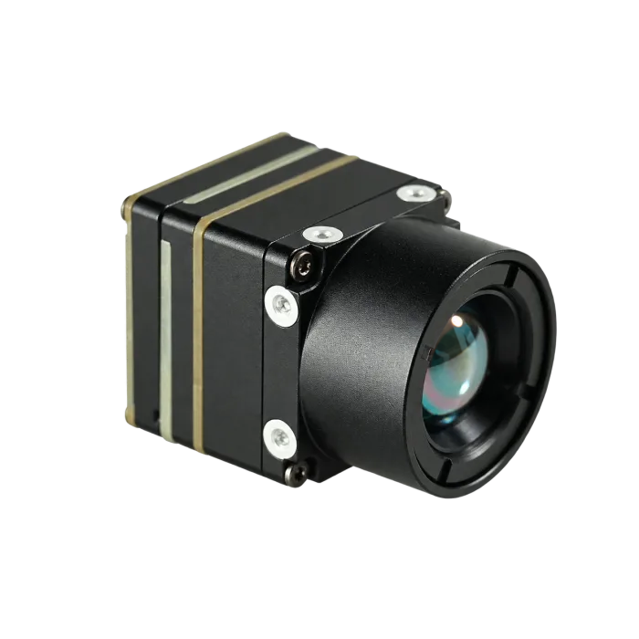
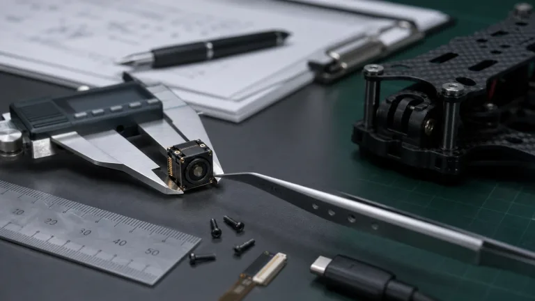
Figure 2: Official AeroMini 640 9 mm module photograph. Confirm the ordered tailboard, cable and full assembly drawing; this photograph does not establish complete assembly dimensions.
CAMCUDA AeroMini 640 Non-Radiometric 9 mm OEM Thermal Imaging Module
The CAMCUDA AeroMini 640 configuration evaluated here pairs a 640 × 512 uncooled VOx detector, 12 μm pixel pitch and a 9 mm F/1.0 lens with the USB + CVBS + MIPI tailboard. Non-radiometric imaging uses a 60 Hz factory default or a 30 Hz factory option; it displays relative thermal patterns without calibrated temperature readings. The selected kit includes a USB cable that requires customer soldering. Confirm each output mode and host format with the matched board and firmware; the factory frame-rate choice does not guarantee simultaneous 60 Hz output on every interface. Use the illustrated 16-pin USB/CVBS and separate 26-pin MIPI/DVP guides for this board: POWER_IN1 and POWER_IN2 are 5 V inputs, and their pin definitions do not apply to the separate Type-C board.
Technical Parameters for OEM Evaluation
| Detector Specifications | |
|---|---|
| Product Model | AeroMini 640 · 9 mm · non-radiometric · USB + CVBS + MIPI |
| Detector Type | Uncooled Vanadium Oxide (VOx) Focal Plane Array |
| Active Array Resolution | 640 × 512 pixels |
| Pixel Pitch | 12 μm |
| Spectral Band | 8 to 14 μm (LWIR) |
| Thermal Sensitivity (NETD) | ≤30 mK @ 25°C, F1.0 |
| Detector Frame Rate | 60 Hz factory default; 30 Hz factory option. Output rate depends on interface, firmware, and host. |
| Optical Configuration | |
| Focal Length | 9 mm, F1.0; selected lens assembly |
| Field of View (FOV) | 48.7° (Horizontal) × 38.6° (Vertical), published lens specification |
| Instantaneous FOV (IFOV) | 1.33 mrad, nominal p/f small-angle estimate |
| Electrical, Interface & Environmental | |
| Video Output Format | USB UVC, CVBS and MIPI available with this interface package; confirm formats and rates for the host |
| Interface Connector | 16-pin USB / CVBS and 26-pin MIPI / DVP connections on the illustrated boards |
| Connector Pinout | Use the matched board diagrams; POWER_IN1 / POWER_IN2 are 5 V inputs. Do not substitute the Type-C or SuperMini pinout. |
| Polarity / Color Palette | White hot / Black hot |
| Supply Voltage Range | Board-dependent; illustrated POWER_IN1 / POWER_IN2 pins: 5 V only, not 12 V |
| Power Consumption | <0.5 W typical at 25°C; complete-kit consumption may differ |
| Operating Temperature Range | -40°C to +80°C |
| Mechanical Shock Tolerance | Confirm the required shock profile for the selected assembly; no rating established by this comparison |
| Weight & Enclosure Envelope | <20 g | 21 × 21 × 28 mm, excluding lens and flange; confirm complete assembly |
Illustrative Pixel-Sampling Ranges (9 mm Lens)
Illustrative geometry using a 1.8 m target height, nominal 12 μm pitch, 9 mm focal length, and the 3 / 12 / 24-pixel assumptions above: R ≈ 1.8 / [N × (0.012 / 9)]. FOV is the published AeroMini lens specification; these sampling ranges are not manufacturer-rated detection, recognition, or identification performance. Use the thermal imaging calculator for IFOV, FOV, and scene coverage; its DRI examples use 1.5 / 6 / 12 pixels, so they do not reproduce this table’s 3 / 12 / 24-pixel assumptions.
| Focal Length | Horizontal × Vertical FOV | 3 pixels (1.5 lp) | 12 pixels (6.0 lp) | 24 pixels (12.0 lp) |
|---|---|---|---|---|
| 9.0 mm | 48.7° × 38.6° | 450 meters | 112.5 meters | 56.25 meters |
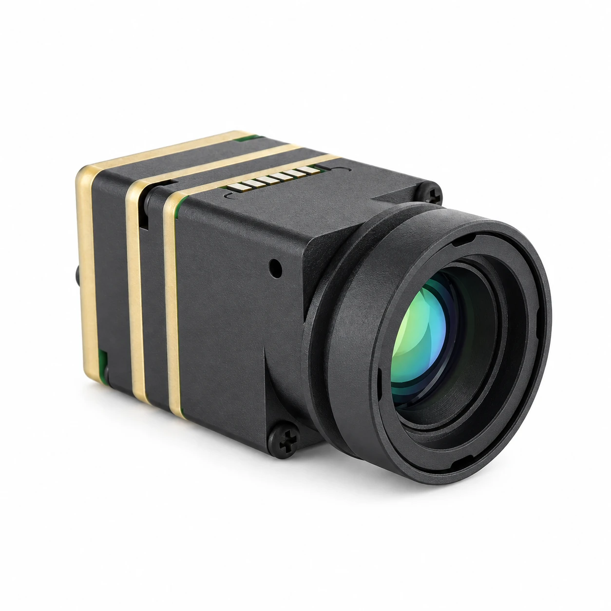
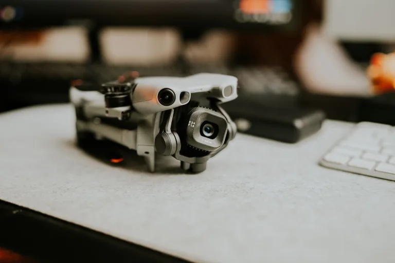
Figure 3: Retained official SuperMini OEM product image. Select the 640 imaging or 640T thermographic model, lens and interface by quotation and the matching datasheet; the picture alone does not identify the delivered configuration or its complete assembly dimensions.
CAMCUDA SuperMini 640 / 640T Ultra-Light LWIR Thermal Camera Module
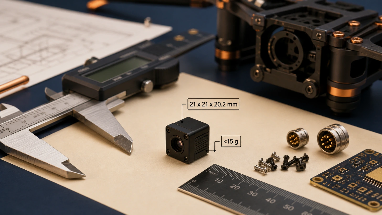
The CAMCUDA SuperMini 640 / 640T Series represents an advancement in SWaP-C thermal engineering, packing a 640 × 512 uncooled VOx focal plane array with an 8 μm pixel pitch into a sub-miniature 13 × 13 × 13.4 mm core weighing less than 3.5 grams. The stated size and weight exclude optics and expansion boards. Operating at typical core power levels of ≤0.5 W at 25°C, excluding the expansion board, this module is engineered for space-critical integrations such as micro-UAV gimbals, robotic end-effectors, helmet-mounted vision systems, and compact handheld inspection tools.
The series is split into two factory-configured hardware variants:
- ⚙️ CAMCUDA SuperMini 640 (Imaging Only): Operates at 50 Hz native frame rate for low-latency visual tracking. Features 8-bit LVCMOS / BT.656 and 2-lane MIPI-CSI-2 visual pipelines. Designed for situational awareness, pilot vision, and FPV navigation.
- ⚙️ CAMCUDA SuperMini 640T (Thermographic / Radiometric): Operates at 30 Hz and outputs calibrated temperature data via CDS3 and radiometric MIPI arrays. Measures absolute surface temperatures across two broad operational ranges (-20°C to +150°C and +100°C to +650°C) with specified accuracy of ±2°C or ±2% of reading at an ambient temperature of -20°C to +60°C. These temperature specifications apply only to the 640T.
Athermal Optical Configuration Options
The listed lens options are specified as F1.0 athermal configurations. Overall dimensions and weight vary with the selected optical assembly.
| Lens Designation | Focal Length | Field of View (H × V) | Aperture | IFOV |
|---|---|---|---|---|
| Wide Angle | 3.7 mm | 90.0° × 68.2° | F1.0 | 2.16 mrad |
| Wide Field | 6.1 mm | 46.6° × 37.6° | F1.0 | 1.31 mrad |
| Balanced Field | 8.7 mm | 40.0° × 32.2° | F1.0 | 0.92 mrad |
| Narrow Field | 11.0 mm | 24.9° × 20.0° | F1.0 | 0.73 mrad |
Electrical Interface & Power Rail Requirements
The bare core uses a Hirose DF40C-30DP-0.4V(51) 30-pin connector and requires all three supply rails below. BT.656 and MIPI cannot operate simultaneously; follow the manual for mating orientation and power-on timing.
| Electrical Path | Operating Voltage / Requirement | Integration & Noise Limits |
|---|---|---|
| MAIN_POWER | 3.8 to 5.2 V DC (Typical 5.0 V) | ≤10 mV p-p maximum ripple noise |
| +3.3 V Power Rail | 3.28 to 3.32 V DC | ≤10 mV p-p maximum ripple noise |
| +1.8 V Power Rail | 1.78 to 1.82 V DC | ≤1 mV RMS noise floor (1 Hz to 50 kHz) |
| Digital Video Output | 8-bit LVCMOS; 2-lane MIPI-CSI-2 | CAMCUDA SuperMini 640: BT.656 | CAMCUDA SuperMini 640T: CDS3 |
| Control Interface | UART Serial (1.8 V logic levels) | TX/RX defined from core perspective |
| USB / CVBS Auxiliary | USB 2.0 pins; Analog CVBS pin | CVBS pin requires external video buffer IC |
Technical author: Daniel · Hardware Support; Sales contributors: Vivian, Lena and Sophie.
8. Frequently Asked Technical Questions
What is the technical difference between Near-Infrared (NIR) imaging and Long-Wave Infrared (LWIR) thermal imaging?
How do uncooled thermal camera modules perform target discrimination in high-temperature ambient environments?
Why do many uncooled microbolometer cores use mechanical shutter calibration (NUC)?
What are the primary integration trade-offs between 8 μm and 12 μm pixel pitch thermal cores?
📚 References & Further Reading
- Industry Standard: EASA Drone Rules and Standards
- Industry Standard: UK CAA Drones
- AeroMini Integration: AeroMini 640 datasheet, matched 16-pin / 26-pin interface references, AeroMini configuration FAQ and AeroMini developer resources. Request documents for the selected board and firmware.
- SuperMini Integration: SuperMini 640 / 640T manual V1.0.0: PDF page 6: 30-pin interface, PDF page 8: power requirements and PDF page 13: bare-core Figure 4.1. These are separate from AeroMini resources.
- Support: CAMCUDA FAQ / Help Center for configuration and document requests.
- Related Guide: Engineering Guide: Choosing a 640×512 Thermal Camera Module for Drone Payloads
- Product Category: CAMCUDA Thermal Observation Devices
- Product Category: CAMCUDA Field Observation Devices