Thermal Imager Cheap vs OEM LWIR Core: Engineering Selection Guide
Thermal Imager Cheap vs OEM LWIR Core: Systems Engineering Selection Guide
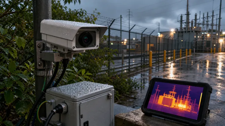
When integrating thermal vision into unmanned platforms, automated inspection rigs, or embedded hardware, procurement teams are frequently tempted by the plummeting upfront cost of consumer-grade thermal sensors. Searching for a thermal imager cheap yields a flooded market of sub-$300 smartphone dongles, entry-level handhelds, and bare-die breakout modules. Here’s the deal: in embedded vision, industrial automation, and aerial instrumentation, a low purchase price almost always hides nasty architectural traps—excessive noise equivalent temperature difference (NETD > 50 mK), wild thermal drift, locked frame rates (≤9 Hz export restrictions), non-standard raw video outputs, and miserable Size, Weight, Power, and Cost (SWaP-C) efficiency.
For optical engineers, roboticists, and payload integrators, the real battle is balancing initial Bill of Materials (BOM) cost against lifecycle integration overhead, spatial resolution, and radiometric accuracy. Moving from a compromised low-cost consumer sensor to a specialized, uncooled Long-Wave Infrared (LWIR) OEM camera core—such as a 640×512 Vanadium Oxide (VOx) microbolometer with a 12 μm or 8 μm pixel pitch—transforms an unstable diagnostic gadget into a deterministic, industrial-grade imaging engine. Look, this guide provides a rigorous systems-engineering breakdown to evaluate when budget sensors suffice, where they fail hard, and how to specify high-performance OEM LWIR cores for mission-critical deployments.
Table of Contents
- 👉 1. The Engineering Trade-offs of Budget Thermal Imagers
- 👉 2. Uncooled LWIR Microbolometer Physics: Pixel Pitch & NETD
- 👉 3. Radiometric Accuracy vs. Qualitative Thermal Contrast
- 👉 4. Low-SWaP Design & Electrical Interface Architectures
- 👉 5. Comprehensive OEM LWIR Core Product Showcases
- 👉 6. Embedded Integration: Power, Thermal Dissipation & Protocol Bridges
- 👉 7. Deep-Dive Engineering FAQ
1. The Engineering Trade-offs of Budget Thermal Imagers
Low-cost thermal imaging solutions minimize manufacturing costs by stripping down detector architecture, optical assemblies, signal processing pipelines, and mechanical housings. While a cheap thermal imager may claim basic infrared functionality on a glossy datasheet, understanding the underlying architectural compromises is essential before finalizing system schematics.
| Engineering Parameter | Budget Consumer Imagers ($150–$400) | OEM Uncooled LWIR Cores ($800–$2,500) |
|---|---|---|
| Native Array Resolution | 80×60 up to 256×192 pixels | 640×512 Native High-Definition Matrix |
| Temporal Output (Frame Rate) | Locked at ≤9 Hz (Export restriction workarounds) | 25 Hz, 30 Hz, 50 Hz, or 60 Hz full rate |
| Pixel Pitch & Active Area | 17 μm to 25 μm (Large, heavy optics) | 12 μm or ultra-compact 8 μm |
| Thermal Sensitivity (NETD) | ≥60 mK to 100 mK (High thermal noise) | ≤40 mK to 50 mK at F/1.0 |
| Embedded Digital Interfaces | Proprietary USB UVC only, high-latency app drivers | MIPI CSI-2, 8-bit LVCMOS, BT.656, RAW14, direct UART |
| Total Cost of Ownership (TCO) | High lifecycle cost (driver rework, thermal drift, custom mounts) | Low lifecycle cost (drop-in SDKs, calibrated LUTs, rugged MTBF) |
1.1 Spatial Resolution and Johnson’s Criteria
Most budget thermal imagers employ focal plane arrays (FPAs) with resolutions ranging from 80×60 to 256×192 pixels. In the shop or on the test range, when evaluating non-destructive testing, building envelope diagnostics, or unmanned aerial vehicle target tracking, native resolution directly dictates the Instantaneous Field of View (IFOV), calculated as:
IFOV = Pixel Pitch (p) / Focal Length (f)
According to classic Johnson’s criteria, spatial resolving power breaks down into clear physical thresholds:
- ⚙️ Detection: Requires 1.5 cycles across target critical dimension (50% probability threshold).
- ⚙️ Recognition: Requires 6.0 cycles across target critical dimension.
- ⚙️ Identification: Requires 12.0 cycles across target critical dimension.
A low-resolution 160×120 sensor paired with a wide 4 mm lens cannot resolve sub-centimeter electronic hotspots or isolate critical structural stress points beyond a couple of meters. A 640×512 native sensor multiplies spatial data density by sixteen times compared to a 160×120 unit. This density enables long-range spatial detection, precise thermal profile modeling, and edge sharpness without forcing platforms to fly or operate dangerously close to high-voltage equipment or hazardous industrial zones.
1.2 Frame Rate Throttling: 9 Hz vs 30/50/60 Hz
Inexpensive thermal devices available on consumer channels are throttled to a locked refresh rate of ≤9 Hz. Manufacturers impose this limit to bypass export classifications without obtaining dual-use export clearances. While 9 Hz is tolerable for inspecting stationary residential circuit panels, it fails completely in dynamic robotics and vision integration:
- ⚙️ UAV Payloads & Gimbals: Angular perturbations cause severe temporal tearing, motion smear, and rolling-shutter artifacts at 9 Hz.
- ⚙️ FPV & Navigation: Latency typically exceeds 120 ms, making closed-loop flight stabilization and obstacle avoidance impossible.
- ⚙️ Machine Vision & Sorting: High-speed industrial sorting lines demand frame rates of ≥30 Hz to 60 Hz to ensure deterministic sub-millisecond trigger synchronization.
Industrial OEM LWIR engines deliver unthrottled factory-configured frame rates of 30 Hz, 50 Hz, or 60 Hz for non-radiometric tracking, alongside stabilized 25 Hz to 30 Hz radiometric video streams. This provides the low-latency temporal response demanded by flight controllers and embedded machine vision pipelines.
1.3 Lens MTF and Optical Transmission
Thermal radiation in the Long-Wave Infrared band (8–14 μm) cannot penetrate standard optical glass. It requires Germanium (Ge) or specialized chalcogenide glass elements. Cheap thermal imagers cut costs by utilizing molded plastic, silicon hybrids, or thin chalcogenide single-element lenses with poor optical transmission (τ < 70%) and high spherical aberrations. These elements severely degrade the overall Modulation Transfer Function (MTF).
Industrial OEM cores leverage precision multi-element anti-reflective (AR) coated Germanium or athermalized chalcogenide lenses with transmission exceeding 92% to 95% at F/1.0 apertures. This maximizes photon collection onto the microbolometer surface, preserving MTF edge sharpness across the entire field of view.
2. Uncooled LWIR Microbolometer Physics: Pixel Pitch & NETD
Modern industrial infrared sensing relies on uncooled Vanadium Oxide (VOx) microbolometer focal plane arrays. VOx technology exhibits a high Temperature Coefficient of Resistance (TCR, typically −2%/K to −3%/K) and superior 1/f flicker noise suppression compared to cheaper Amorphous Silicon (α-Si) arrays.
In a VOx microbolometer, incoming 8–14 μm radiation is focused through an AR-coated Germanium lens onto a micro-machined bridge suspended over a silicon Readout Integrated Circuit (ROIC). The absorbed thermal photon flux increases the temperature of the VOx layer, altering its electrical resistance. The underlying ROIC digitizes these resistance shifts at high speed, passing the signal to an on-core digital processing engine for 2-point Non-Uniformity Correction (NUC), dead pixel replacement, and spatial filtering.
2.1 The Transition: 17 μm to 12 μm and 8 μm VOx Arrays
Standard legacy thermal detectors relied on 17 μm pixel pitch architectures. Advances in semiconductor MEMS fabrication have made 12 μm and ultra-miniature 8 μm architectures commercially viable:
- ✅ Optical Aperture & Weight Reduction: Transitioning from 17 μm to 8 μm reduces the focal length required to achieve an identical Field of View (FOV) by more than 50%. Shorter focal lengths allow the use of significantly smaller lens diameters, decreasing overall optical payload weight and volume by up to 70%.
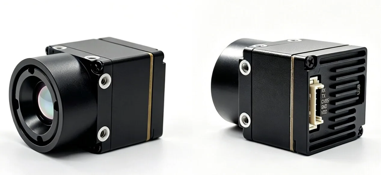
- ✅ Ultra-Low SWaP Footprint: An 8 μm 640×512 core can achieve a chassis footprint of just 13×13×13.4 mm and weigh under 3.5 grams, making it suitable for micro-gimbals, soldier-worn systems, and sub-250-gram UAV platforms.
2.2 Thermal Sensitivity (NETD) and Signal-to-Noise Ratio (SNR)
Noise Equivalent Temperature Difference (NETD) is the primary metric of thermal sensitivity, denoting the temperature change that produces an electrical signal equivalent to the detector’s internal noise floor. It is calculated as:
NETD = (4 · F² · V_n) / (τ_o · A_d · (dV/dT) · (dL/dT))
Where F is optical F-number, V_n is total noise voltage, τ_o is optical transmission, A_d is active pixel area, and dL/dT is the derivative of blackbody radiance in the 8–14 μm spectral band. While cheap sensors often feature NETD values between 60 mK and 100 mK at 25°C—resulting in noisy, low-contrast imagery under overcast or maritime conditions—industrial OEM LWIR cores achieve ≤50 mK or optional ≤40 mK at F/1.0. This low noise floor is critical for ASNT Thermal/Infrared Testing standards, revealing minute structural anomalies and thermal leakage.
2.3 Non-Uniformity Correction (NUC) and Thermal Drift
Due to micro-scale MEMS manufacturing tolerances, every bolometer pixel displays slight variations in baseline resistance and thermal responsivity, causing Fixed Pattern Noise (FPN). Cheap thermal units often use rudimentary mechanical shutters that freeze video unpredictably every few seconds, or lack dynamic temperature-dependent offset mapping altogether.
OEM-grade cores implement factory-calibrated look-up tables (LUTs) spanning −40°C to +80°C. These algorithms perform real-time continuous background compensation, minimizing calibration interruptions and maintaining clean radiometric outputs during rapid ambient transitions.
3. Radiometric Accuracy vs. Qualitative Thermal Contrast
Systems engineers must choose between qualitative imaging cores and fully radiometric thermographic modules based on their application requirements.
| Operational Category | Qualitative Thermal Core (e.g., AeroMini / SuperMini 640) | Full Radiometric Core (e.g., SuperMini 640T) |
|---|---|---|
| Output Data Format | 8-bit display video (YUV, BT.656, CVBS, White-Hot/Black-Hot) | 14-bit/16-bit per-pixel linear digital temperature arrays (RAW / CDS3) |
| Dynamic Processing | Auto Gain Control (AGC) & dynamic histogram equalization | Calibrated linear radiometric temperature mapping equations |
| Measurement Range | N/A (Visual contrast mapping only) | −20°C to +150°C (High Gain), +100°C to +650°C (Low Gain) |
| Application Scope | FPV flying, perimeter security, search & rescue, optical tracking | Solar panel inspection, utility substation health, structural NDT |
3.1 Absolute Temperature Calibration Pipeline
A qualitative core applies continuous AGC algorithms to distribute 256 grayscale levels across the warmest and coolest points in the scene. While this maximizes visual contrast for a human operator, it destroys the physical correlation between digital pixel values and absolute temperatures.
A radiometric core preserves the underlying 14-bit ADC values, applying real-time corrections based on internal temperature sensors located at the FPA substrate, housing, and lens barrel:
T_target = f(DN_pixel, T_FPA, T_housing, ε, Distance, Atmospheric_tau)
Cheap thermal gadgets frequently suffer from thermal drift exceeding ±10°C as ambient temperatures change. Industrial OEM cores maintain calibrated accuracies within ±2°C or ±2% across standard operating ranges, providing the reliability required for predictive maintenance.
3.2 Dynamic Range, Gain States, and High-Temperature Measurement
Radiometric cores utilize dual-gain architectures:
- ⚙️ High-Gain State: Optimized for low-temperature observation (−20°C to +150°C), maximizing sensitivity to resolve subtle thermal deltas.
- ⚙️ Low-Gain State: Configures the ROIC integration capacitors to prevent saturation when imaging high-temperature industrial equipment, furnaces, or electrical arcs (+100°C to +650°C).
4. Low-SWaP Design & Electrical Interface Architectures
Size, Weight, Power, and Cost (SWaP-C) optimization is critical for embedded vision. In aerial robotics, every single gram of payload weight cuts flight endurance directly out of your battery budget. Legacy industrial cameras weighing 200–400 grams demand heavy gimbals and bulky battery packs.
Modern uncooled OEM cores solve these physical bottlenecks through ultra-dense component packaging, low-power ROICs (≤0.5 W), and flexible physical interfaces. For broader platform options, integrators can explore specialized uncooled thermal modules designed for micro-gimbals and industrial hardware.
4.1 Digital vs Analog Transport: MIPI, LVCMOS, BT.656, and USB
Budget thermal units generally rely on USB UVC video running through consumer mobile apps, introducing 80–150 ms of software-induced latency. OEM LWIR cores provide direct physical-layer connections for embedded SoCs:
- ⚙️ 2-Lane MIPI CSI-2: Connects directly to embedded Application Processors (e.g., NVIDIA Jetson Orin, NXP i.MX8, Raspberry Pi CM4) with sub-frame pipeline latency (<10 ms).
- ⚙️ 8-bit LVCMOS / BT.656: Feeds uncompressed digital video straight into FPGAs or DSPs for real-time edge AI inference and object tracking.
- ⚙️ Native Analog CVBS (PAL/NTSC): Enables direct transmission over analog 5.8 GHz video links for zero-latency FPV piloting.
- ⚙️ Modular USB Expansion Boards: Bridges such as the TMS6102V100F022 convert high-density board-to-board connectors to standard USB for rapid prototyping.
5. Comprehensive OEM LWIR Core Product Showcases
The following product showcases provide verified technical specifications, electrical requirements, and optical field-of-view matrices for two industry-standard uncooled LWIR OEM cores designed for UAV payloads and embedded systems.
CAMCUDA AeroMini 640×512 Uncooled LWIR USB Thermal Camera Core
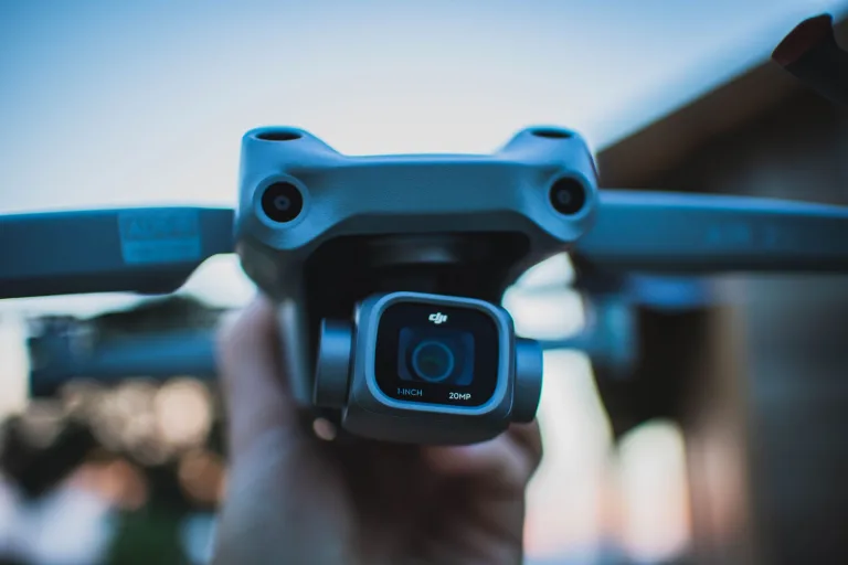
The CAMCUDA AeroMini 640 is an uncooled Long-Wave Infrared core designed for UAV payloads, DJI-type drone platforms, multi-axis gimbals, and embedded inspection hardware. Built around a 640×512 uncooled VOx focal plane array with a 12 μm pixel pitch, the AeroMini 640 delivers thermal sensitivity (≤50 mK standard, ≤40 mK optional at F/1.0) in a bare chassis weighing under 20 grams. The core features a factory default frame rate of 60 Hz (with an optional 30 Hz ordering configuration) for non-radiometric imaging, alongside a 25 Hz radiometric variant covering temperature spans from −20°C to +550°C.
AeroMini 640 Technical Specifications
| Parameter | Specification | Configuration Notes |
|---|---|---|
| Array Resolution | 640 × 512 pixels | Both imaging and radiometric variants |
| Detector Material | Vanadium Oxide (VOx) | Uncooled microbolometer FPA |
| Pixel Pitch | 12 μm | 8–14 μm LWIR spectral response |
| Frame Rates | 60 Hz default / 30 Hz factory option | Radiometric version runs at 25 Hz |
| Sensitivity (NETD) | ≤50 mK at 25°C, F/1.0 | Optional ≤40 mK high-sensitivity build |
| Supply Voltage & Power | 5 V or 12 V (board-dependent) | Typical core power consumption <0.5 W at 25°C |
| Digital Video Formats | YUV, USB, BT.656 | Interface board and firmware dependent |
| Analog Video Formats | CVBS, PAL, NTSC | Selectable via hardware expansion |
| Serial Communication | UART, RS232, RS422 | Core command and control protocol |
| Dimensions & Weight | 21 × 21 × 28 mm | <20 g | Excludes lens and flange mounts |
| Thermographic Range | −20°C to +550°C | Applies strictly to radiometric version |
| Operating Temperature | −40°C to +80°C | Storage: −50°C to +85°C; Humidity 5–95% non-cond. |
AeroMini 640 Lens & Field of View Matrix
| Focal Length | Field of View (H × V) | Camera Model Compatibility |
|---|---|---|
| 4 mm | 100° × 82° | Non-radiometric imaging |
| 7 mm | 64° × 52° | Non-radiometric imaging |
| 9 mm | 48.7° × 38.6° | Non-radiometric & Radiometric option |
| 13 mm | 31.9° × 25.7° | Non-radiometric & Radiometric option |
| 15 mm | 29.3° × 23.5° | Enquiry configuration |
| 18 mm | 24.2° × 19.5° | Non-radiometric & Radiometric option |
| 25 mm | 17.5° × 14° | Non-radiometric imaging |
| 35 mm | 12.5° × 10° | Non-radiometric imaging |
| 50 mm | 8.8° × 7.0° | Non-radiometric narrow telephoto |
CAMCUDA SuperMini 640 / 640T Ultra-Light LWIR Thermal Camera Module
The CAMCUDA SuperMini 640 / 640T series is an ultra-miniature LWIR module designed for micro-gimbals, soldier systems, FPV drones, and SWaP-constrained industrial vision platforms. Leveraging an uncooled VOx detector with a sub-micron 8 μm pixel pitch, the SuperMini core measures 13×13×13.4 mm and weighs less than 3.5 grams. The series offers two factory configurations: the SuperMini 640 (50 Hz imaging core with 8-bit LVCMOS/BT.656 and 2-lane MIPI) and the SuperMini 640T (30 Hz thermographic core supporting per-pixel CDS3/MIPI radiometric temperature streaming).
SuperMini 640 vs 640T Architectural Differences
| Functional Feature | SuperMini 640 (Imaging Only) | SuperMini 640T (Thermographic) |
|---|---|---|
| Frame Rate | 50 Hz high-speed video | 30 Hz radiometric video |
| Temperature Measurement | No (Visual thermal imaging only) | Yes (−20°C to +150°C & +100°C to +650°C) |
| Digital Data Protocol | 8-bit LVCMOS / BT.656, 2-lane MIPI | CDS3 temperature-data paths, 2-lane MIPI |
| Target Application | Low-latency tracking, FPV, optical payloads | Quantitative thermography, predictive maintenance |
SuperMini 640 / 640T Electrical & Mechanical Specifications
| Parameter / Rail | Requirement | Integration Note |
|---|---|---|
| Resolution & Pixel Pitch | 640 × 512 | 8 μm VOx | 8–14 μm spectral range, NETD ≤40 mK @ 25°C, F1.0 |
| Core Dimensions & Mass | 13 × 13 × 13.4 mm | <3.5 g | Bare core excluding lens and expansion board |
| MAIN_POWER Rail | 3.8 V to 5.2 V (Typical 5.0 V) | 10 mV peak-to-peak maximum allowable noise |
| +3.3 V Internal Rail | 3.28 V to 3.32 V | 10 mV peak-to-peak maximum noise |
| +1.8 V Internal Rail | 1.78 V to 1.82 V | 1 mV RMS maximum noise (1 Hz to 50 kHz bandwidth) |
| Typical Core Power | ≤0.5 W | Measured at 25°C steady state |
| Interface Connector | Hirose DF40C-30DP-0.4V(51) | 30-pin board-to-board high-density connector |
| Control Interface | UART (1.8 V logic levels) | TX/RX defined from core perspective |
| Analog Video (CVBS) | Dedicated CVBS pin | Requires external video buffer IC on carrier board |
| Expansion Board Option | TMS6102V100F022 | Provides 4-pin USB connection for 640 & 640T |
SuperMini 640 / 640T Athermal Optical Configurations
| Focal Length | Aperture | Field of View (H × V) | IFOV |
|---|---|---|---|
| 3.7 mm | F1.0 Athermal | 90.0° × 68.2° (Wide Angle) | 2.16 mrad |
| 6.1 mm | F1.0 Athermal | 46.6° × 37.6° (Wide Field) | 1.31 mrad |
| 8.7 mm | F1.0 Athermal | 40.0° × 32.2° (Balanced Field) | 0.92 mrad |
| 11.0 mm | F1.0 Athermal | 24.9° × 20.0° (Narrow Field) | 0.73 mrad |
For complete 3D mechanical CAD STEP models, electrical interface pinouts, and SDK documentation, access the CAMCUDA Support Downloads directory.
6. Embedded Integration: Power, Thermal Dissipation & Protocol Bridges
Integrating an OEM LWIR core into a rugged embedded platform requires close attention to power supply integrity and thermal management.
6.1 Power Rail Noise and Filtering
VOx microbolometers and their integrated Readout Integrated Circuits (ROICs) process low-level analog micro-volt signals before on-chip digitization. High-frequency noise on the power rails converts directly into spatial banding, grain, and flickering artifacts:
- ⚙️ Main Power Rail (3.8 V to 5.2 V): Must maintain ripple below 10 mV peak-to-peak. Use low-ESR ceramic bypass capacitors paired with ferrite beads located close to the Hirose connector pins.
- ⚙️ Internal +1.8 V Rail: Sensitive to high-frequency jitter, requiring a low-noise, high-PSRR linear regulator maintaining noise below 1 mV RMS across the 1 Hz to 50 kHz spectrum.
- ⚙️ Ground Isolation: Maintain separate analog return paths and high-speed digital return paths (MIPI / LVCMOS) back to a single star ground point on the carrier board to prevent return currents from modulating detector bias voltages.
6.2 Thermal Sinking and Enclosure Geometry
Uncooled microbolometer cores continuously dissipate approximately 0.5 W of thermal energy during steady-state operation. If heat builds up inside an enclosed chassis, internal temperatures will rise, drifting outside optimal calibration bands and inducing measurement offsets.
- ⚙️ Conductive Heat Paths: In sealed IP67 housings, provide a mechanical conduction path using a thermal interface pad (thermal conductivity k ≥ 3.0 W/m·K) connecting the core chassis directly to the outer aluminum enclosure.
- ⚙️ Avoid Localized Gradients: Ensure high-power processing units (e.g., companion computers, motor ESCs) are isolated from the optical barrel to prevent asymmetric thermal gradients across the Germanium lens, which can cause severe vignetting and corner defocusing.
For technical application notes on custom carrier board routing and optical housing design, visit the CAMCUDA Engineering Blog.
7. Deep-Dive Engineering FAQ
Why do sub-$300 budget thermal imagers fail to meet industrial and OEM integration standards?
Can a cheap thermal imager perform calibrated, quantitative radiometric temperature measurement?
What are the hidden lifecycle costs of using consumer thermal modules instead of OEM cores?
📚 References & Further Reading
- Industry Standard: ASNT Thermal/Infrared Testing Guidelines
- Aerospace & Defense Reference: Wikipedia – Unmanned Aerial Vehicle Payload Standards
- Engineering Resource: CAMCUDA Engineering Blog: Low-SWaP Thermal Integration
- SDKs & Technical Manuals: CAMCUDA Support Downloads & Datasheets
- Product Catalog: CAMCUDA Uncooled LWIR Core Modules