Affordable Infrared Camera Modules: B2B OEM & Integration Guide
Engineering an automated inspection line, embedded building sensor, continuous process monitor, or aerial vision payload has historically forced system architects into an expensive compromise. On one end of the spectrum sit high-end scientific thermal cores whose prohibitive initial bill-of-materials (BOM) costs make multi-node deployment economically impossible; on the other sit consumer-grade smartphone dongles and hobbyist breakout boards that lack industrial reliability, dynamic thermal stability, deterministic bus timing, and robust mechanical packaging. Sourcing an affordable infrared camera module for commercial, industrial, and original equipment manufacturer (OEM) environments requires evaluating uncooled Long-Wave Infrared (LWIR) detector physics, wafer-level packaging (WLP) manufacturing economics, optical aperture scaling, and native board-level communication interfaces that eliminate unnecessary protocol bridge chips, proprietary interface adapters, and custom driver overhead.
Here’s the deal: true hardware affordability in thermal vision engineering is never defined by the unit purchase price of a sensor component alone. In the shop and on the bench, what matters is the Total Cost of Ownership (TCO) across the entire product lifecycle. That means factoring in optical customization costs, embedded compute overhead, power conditioning footprint, mechanical integration simplicity, and long-term radiometric drift calibration. When engineering teams select modern uncooled Vanadium Oxide (VOx) focal plane arrays (FPAs) engineered with standardized serial and parallel communication buses, they can deploy compact 160×120 thermal nodes for continuous localized condition monitoring or scale up to ultra-high-definition 1280×1024 thermal imaging matrices for long-range unmanned aerial vehicle (UAV) payloads without breaking project budgets.
This comprehensive engineering guide examines the foundational physical principles, digital interface architectures, optical design calculations, and on-device computational pipelines required to integrate cost-effective LWIR thermal camera modules directly into custom embedded hardware. Integrators evaluating completed handheld instruments alongside modular bare-board sub-assemblies can reference our in-depth handheld thermal imaging camera field buying guide, explore the latest industrial imaging innovations across the CAMCUDA engineering blog, or review production-ready systems via the complete CAMCUDA infrared catalog.
Table of Contents
- 👉 1. True Affordability in LWIR Engineering: Breaking Down Cost Drivers
- 👉 2. Spectral Differentiation: LWIR Microbolometers vs. Budget NIR/SWIR Systems
- 👉 3. Embedded Bus Protocols & Hardware Interface Architectures
- 👉 4. Edge AI Integration & On-Device Thermal Computer Vision
- 👉 5. SWaP-C Optimization for Drone Payloads & Embedded IoT Systems
- 👉 6. High-Resolution OEM Engineering Deep-Dive: CAMCUDA HR-1280
- 👉 7. Ultra-Compact Embedded Core Deep-Dive: CAMCUDA TC160-NF
- 👉 8. Comparative Engineering Showcase: CAMCUDA OEM Module Specifications
- 👉 9. Step-by-Step OEM Integration & RFQ Procurement Checklist
- 👉 10. Deep-Dive Technical FAQ
1. True Affordability in LWIR Engineering: Breaking Down Cost Drivers
The economic landscape of thermal infrared imaging has transformed radically over the past two decades. Historically, infrared systems relied on cryogenically cooled photon detectors—such as Indium Antimonide (InSb) or Mercury Cadmium Telluride (MCT)—operating within Mid-Wave Infrared (MWIR, 3–5 µm) or Long-Wave Infrared (LWIR, 8–14 µm) regimes. These cooled systems required closed-cycle Stirling mechanical cryocoolers to drop focal plane temperatures to 77 Kelvin (-196°C). The precision mechanical moving parts, helium gas hermetic seals, and severe thermal insulation requirements created devices with unit prices exceeding tens of thousands of dollars and mean-time-between-failures (MTBF) limited to several thousand operating hours.
Modern commercial, industrial, and embedded imaging systems rely predominantly on uncooled microbolometer technology. An uncooled thermal detector consists of a two-dimensional focal plane array of microscopic thermal sensing elements fabricated directly above a silicon Readout Integrated Circuit (ROIC). Rather than directly exciting electrons into conduction bands via incoming high-energy photons, microbolometer elements absorb incident infrared thermal flux, experience a minute rise in internal physical temperature, and alter their electrical resistance. This electrical resistance change is measured by the underlying ROIC and converted into calibrated digital signal counts. Within this framework, modern hardware affordability is governed by four interconnected engineering factors:
- ⚙️ Active Sensing Material and Fab Yields: Microbolometers are primarily manufactured from either Amorphous Silicon (a-Si) or Vanadium Oxide (VOx). While a-Si offered early cost advantages due to standard silicon foundry process compatibility, VOx has established itself as the industrial benchmark. VOx exhibits a significantly higher Temperature Coefficient of Resistance (TCR), providing superior thermal sensitivity—frequently achieving Noise Equivalent Temperature Difference (NETD) values of ≤35 mK—while operating at lower bias voltages. Maturation in thin-film VOx deposition and micro-machining lithography has increased fabrication yields, drastically lowering the raw sensor core BOM cost.
- ⚙️ Wafer-Level Packaging (WLP) vs. Traditional Metallic Hermetic Cans: In traditional thermal core manufacturing, each diced microbolometer FPA was seated inside a dedicated, machined metallic or ceramic vacuum package featuring a single-crystal Germanium window, pumped down to deep vacuum, and sealed using metal pinch-off tubes. In contrast, modern WLP processes align and bond an entire silicon window wafer directly to the detector wafer in a high-vacuum chamber prior to dicing. This automated batch packaging technique reduces package volume by up to 80%, cuts physical material costs, and enables microbolometer modules to achieve sub-hundred-dollar cost points at volume.
- ⚙️ Pixel Pitch Scaling and Optical Element Sizing: Shrinking the detector pixel pitch from legacy 35 µm and 25 µm dimensions down to 17 µm and 12 µm directly contracts the physical diagonal size of the focal plane array. Optical physics dictates that the physical diameter and focal length of an infrared objective lens are directly proportional to the active sensor dimensions for a given target Field of View (FOV). Because single-crystal Germanium (Ge) and Chalcogenide infrared glass elements represent between 30% and 50% of a completed thermal module’s hardware cost, reducing the required optical clear aperture yields substantial BOM savings.
- ⚙️ Integration Simplicity and Standardized Digital Busses: A low-cost sensor core that requires a dedicated FPGA companion chip, specialized power rail sequencing, analog anti-aliasing filters, and proprietary frame grabbers will inevitably produce an expensive final system. True hardware economy demands thermal camera modules equipped with native digital video outputs (BT.656, BT.1120, SDI, CameraLink) or direct embedded bus lines (SPI, USB, UART), allowing direct routing to host ARM, RISC-V, or x86 microprocessors.
2. Spectral Differentiation: LWIR Microbolometers vs. Budget NIR/SWIR Systems
Look, system integrators evaluating an affordable infrared camera frequently run into confusion regarding spectral operational bands. Marketing teams love labeling simple visible-light CMOS sensors with active LED spotlights as “infrared cameras.” But on the shop floor, low-cost Near-Infrared (NIR) and Short-Wave Infrared (SWIR) sensors operate under optical and physical mechanisms that differ fundamentally from true Long-Wave Infrared (LWIR) microbolometers.
The electromagnetic spectrum governs how different sensors observe the physical environment:
- ✅ Visible Spectrum (0.4 µm to 0.7 µm): Conventional CMOS/CCD imaging systems capture reflected visible photons generated by ambient sunlight or artificial illumination.
- ✅ Near-Infrared (NIR, 0.75 µm to 1.0 µm): Standard silicon CMOS image sensors maintain weak spectral sensitivity extending into the NIR range. Low-cost “night vision” cameras achieve night-time capability simply by removing the mechanical IR-cut filter and activating high-power 850 nm or 940 nm infrared Light Emitting Diodes (LEDs). These systems rely purely on reflected light; in absolute zero-lux darkness without active illuminators, they produce zero signal. In the field, NIR sensors cannot measure temperature, detect thermal leakage, or penetrate thick industrial smoke or dust.
- ✅ Short-Wave Infrared (SWIR, 1.0 µm to 1.7 µm): SWIR imaging typically requires Indium Gallium Arsenide (InGaAs) photodiode arrays. SWIR systems capture both reflected photons and specialized laser illumination, enabling penetration through atmospheric haze, silicon wafer inspection, and chemical spectroscopy. However, InGaAs fabrication remains complex and expensive, positioning SWIR modules well outside budget-constrained OEM architectures.
- ✅ Long-Wave Infrared (LWIR, 8.0 µm to 14.0 µm): True thermal imaging operates in the LWIR spectrum. At these wavelengths, sensors do not detect reflected ambient light; instead, they capture direct thermal electromagnetic radiation emitted by all objects possessing a physical temperature above absolute zero (0 Kelvin / -273.15°C).
This emission phenomenon is governed mathematically by Planck’s Radiation Law and the Stefan-Boltzmann Law, which states that the total radiant energy emitted per unit surface area of a blackbody per unit time ($j^*$) is directly proportional to the fourth power of the thermodynamic temperature ($T$):
j* = ε σ T4
Where ε represents the surface emissivity of the observed target, σ is the Stefan-Boltzmann constant (5.670374 × 10⁻⁸ W/m2K4), and $T$ is absolute temperature in Kelvin. Because LWIR microbolometers detect emitted thermodynamic radiation, an affordable uncooled VOx thermal module operates in absolute zero-lux darkness, penetrates heavy industrial smoke, fog, and obscurants, and outputs quantitative radiometric temperature data for every spatial pixel across the scene.
3. Embedded Bus Protocols & Hardware Interface Architectures
The electrical and communication interface between an uncooled thermal core and the host embedded compute platform dictates processing latency, system bill-of-materials, PCB layer counts, and firmware complexity. System designers must match data throughput demands against host controller pin counts and bandwidth capabilities.
For compact, lower-resolution thermal modules (such as 160×120 pixel arrays operating at up to 25 FPS), the Serial Peripheral Interface (SPI) is an optimal low-cost, low-pin-count interconnect. In high-speed master mode (typically running at clock frequencies between 12 MHz and 32 MHz), the thermal module streams 14-bit or 16-bit raw radiometric pixel words directly into the host microcontroller memory using Direct Memory Access (DMA). This architecture allows resource-constrained microcontrollers—such as ARM Cortex-M4, Cortex-M7, or ESP32 series—to ingest real-time thermal matrices without requiring a dedicated external memory controller or high-speed video capture peripheral.
When stepping up to high-resolution thermal imaging modules (such as 1280×1024 arrays operating at 50 Hz), data bandwidth jumps substantially. A 1280×1024 sensor streaming 16-bit uncompressed frames at 50 FPS produces a raw throughput exceeding 1.04 Gbps:
1280 × 1024 pixels × 16 bits/pixel × 50 frames/sec ≈ 1,048,576,000 bits/sec (1.048 Gbps)
To transport this bandwidth reliably without dropping frames or overloading host processors, high-performance OEM modules utilize specialized parallel and serialized digital video protocols:
- ⚙️ BT.656 and BT.1120 Parallel Video Buses: These standardized digital video standards multiplex timing synchronization signals (Start of Active Video / End of Active Video codes) directly onto clock and parallel data lines. This enables direct hardware connection to the Camera Interface (CAMIF) or Video Input Subsystem of embedded application processors like the NXP i.MX8, Rockchip RK3588, or NVIDIA Jetson family without bridge ICs.
- ⚙️ Serial Digital Interface (SDI) and CameraLink: For industrial automation racks, machine vision cells, or unmanned aerial vehicle (UAV) camera gimbals requiring long-distance transmission, SDI and CameraLink provide deterministic, low-latency serialized output streams over coaxial cabling or low-voltage differential signaling (LVDS) harnesses.
- ⚙️ Industrial Serial Telemetry (RS-232 / RS-485 / RS-422): While high-speed digital buses carry raw or processed video frames, control and command telemetry channels are isolated to robust serial links. Standardized UART/RS-485 commands allow host control of Non-Uniformity Correction (NUC) shutter calibration cycles, digital zoom scaling, radiometric gain mode switching, and pseudo-color palette Look-Up Table (LUT) mapping.
4. Edge AI Integration & On-Device Thermal Computer Vision
Pairing low-cost infrared modules with distributed edge computing architectures enables autonomous anomaly detection, machine safety shutoff, structural heat loss monitoring, and persistent security surveillance without relying on high-latency cloud processing. Processing thermal data directly at the edge minimizes network bandwidth consumption, prevents sensitive facility data from leaving the local perimeter, and delivers sub-millisecond deterministic decision-making. Integrators deploying distributed intelligence frameworks can review the foundational principles of Wikipedia – Edge Computing to structure optimal system topologies.
In practice, running deep learning models on thermal data streams requires dedicated digital preprocessing. Standard computer vision models trained on RGB imagery (such as standard ImageNet weights) perform poorly when fed raw microbolometer data. A robust thermal edge pipeline consists of four sequential processing stages:
- ⚙️ Stage 1: Raw Readout & Bad Pixel Replacement (BPR): Microbolometer manufacturing yields occasionally produce non-responsive or outlier pixels. The host processing pipeline identifies these static locations and replaces them in real time using 2D bilinear interpolation from adjacent healthy detector pixels.
- ⚙️ Stage 2: Non-Uniformity Correction (NUC) & Drift Compensation: Because individual VOx microbolometer elements drift slightly in response to internal thermal ambient fluctuations, 2-point calibration offset and gain matrices stored in module non-volatile memory are continuously applied to balance the frame.
- ⚙️ Stage 3: Dynamic Range Compression (AGC & CLAHE): Microbolometers output high-dynamic 14-bit or 16-bit linear radiometric counts (representing thousands of temperature gradations). Neural network inference engines require 8-bit [0, 255] normalized tensors. Embedded systems utilize Contrast Limited Adaptive Histogram Equalization (CLAHE) or platform-optimized Automatic Gain Control (AGC) algorithms to compress dynamic range while accentuating subtle thermal edge boundaries.
- ⚙️ Stage 4: Model Inference on Embedded NPUs: Compressed single-channel 8-bit thermal matrices are fed into lightweight convolutional or transformer architectures (such as MobileNetV3, YOLOv8-Nano, or custom autoencoders) optimized using open-source frameworks like TensorFlow Lite, ONNX Runtime, or TensorRT to execute real-time thermal object tracking and automated thermal threshold classification.
5. SWaP-C Optimization for Drone Payloads & Embedded IoT Systems
Deploying thermal vision into field-ready commercial products requires strict adherence to Size, Weight, Power, Cost, and Performance (SWaP-C) constraints. The engineering tradeoffs differ fundamentally between airborne UAV payload applications and stationary building automation or smart appliance nodes.
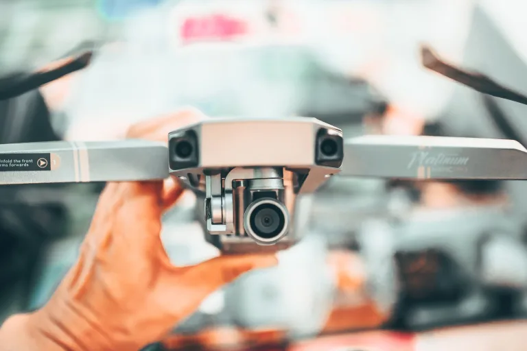
For aerial drone payloads, mass is the most critical constraint. Every additional gram carried in an aerial gimbal reduces battery runtime and cuts flight endurance. High-resolution uncooled cores designed for airborne integration—such as the CAMCUDA HR-1280—minimize bare module mass to just 68 grams within a 35×35×35 mm physical enclosure. This low mass profile allows 3-axis brushless micro-gimbals to remain well under standard commercial 250-gram payload ceilings. Wide input voltage ranges (5 V to 24 V DC) allow the module to be powered directly from main multi-cell LiPo flight batteries via standard distribution boards, eliminating heavy dedicated buck/boost converters and reducing electromagnetic interference (EMI).
For stationary Internet of Things (IoT) devices, smart HVAC monitors, and embedded industrial appliances, thermal dissipation and electrical power budget dominate system design. In these applications, ultra-compact modules—such as the CAMCUDA TC160-NF—operate on a single 3.3 V DC rail with an ultra-low power consumption of approximately 76 mW to 78 mW. This low power profile allows the module to be integrated into space-constrained housings without active cooling fans and prevents module self-heating from creating radiometric measurement drift across the detector array.
6. High-Resolution OEM Engineering Deep-Dive: CAMCUDA HR-1280
The CAMCUDA HR-1280 is an uncooled LWIR thermal imaging core engineered for applications requiring high spatial resolution, extensive optical flexibility, and versatile digital interface options. Built on an uncooled Vanadium Oxide (VOx) focal plane array, the HR-1280 delivers a native resolution of 1280×1024 pixels with a 12 µm pixel pitch, operating across the standard 8 to 14 µm spectral response band.
With an NETD of ≤35 mK at 25°C with an F1.0 optical aperture, the HR-1280 resolves subtle thermal gradients in low-contrast environments. Operating at a full 50 Hz frame rate, it captures dynamic scenes without spatial motion blur, making it suitable for aerial drone payloads, machine vision inspection lines, long-range perimeter security, and OEM thermal devices. The module features a compact 35×35×35 mm form factor and a bare weight of 68 grams (without lens), supporting a wide 5 V to 24 V DC power input range.
Digital video integration is supported through multiple output paths, including BT.656, BT.1120, SDI, and CameraLink, while command and control are managed via industrial RS-232, RS-485, or RS-422 serial links. A comprehensive suite of interchangeable objective lenses—including 9 mm, 13 mm, 19 mm, 25 mm, 35 mm, 50 mm, 75 mm, and 100 mm focal lengths—allows engineering teams to match the system’s Field of View and Detection, Recognition, and Identification (DRI) capabilities to specific project requirements. (Note: CVBS analog video is not natively supported in the standard configuration; NDAA compliance statements are available upon request).
| Specification Parameter | Technical Rating / Preserved Value |
|---|---|
| Detector Type | Uncooled VOx (Vanadium Oxide) |
| Array Resolution | 1280 × 1024 pixels |
| Pixel Pitch | 12 μm |
| Spectral Response Band | 8 – 14 μm (LWIR) |
| Frame Rate | 50 Hz |
| Thermal Sensitivity (NETD) | ≤ 35 mK @ 25°C, F#1.0 |
| Lens Focal Length Options | 9 / 13 / 19 / 25 / 35 / 50 / 75 / 100 mm |
| Input Voltage Range | 5.0 V – 24.0 V DC |
| Digital Video Output | BT656 / BT1120 / SDI / CameraLink |
| Control Communication | RS232 / RS485 / RS422 |
| Module Bare Weight | 68 g (Without lens) |
| Physical Dimensions | 35 × 35 × 35 mm (Without lens) |
View Product Details & Pricing ➔
7. Ultra-Compact Embedded Core Deep-Dive: CAMCUDA TC160-NF
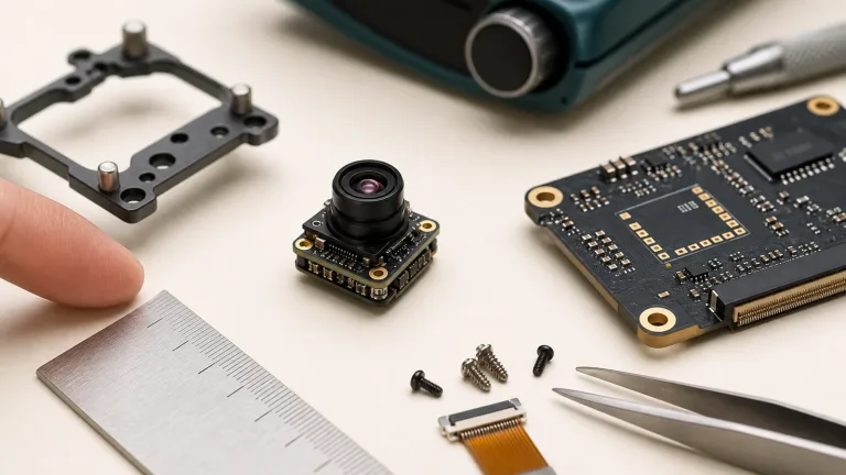
The CAMCUDA TC160-NF (SKU: MI1602M5S) is an ultra-compact uncooled LWIR thermal imaging core engineered for high-volume OEM integration, embedded sensing nodes, smart building automation, HVAC performance monitoring, and edge AI vision devices. Designed for direct host-board integration, the TC160-NF delivers a native resolution of 160×120 pixels (19,200 active radiometric measurement points) across the 8 to 14 µm spectral band.
Operating at a frame rate of up to 25 FPS, the TC160-NF features a narrow Field of View fixed optical configuration (56° Diagonal, 45° Horizontal, 34° Vertical), providing concentrated scene coverage without requiring external focusing mechanisms. The module is engineered for ultra-low power consumption, drawing approximately 76 mW to 78 mW from a single 3.3 V DC supply. Communication and high-speed data transfer are handled over a host SPI bus routed through an ultra-thin 10-pin Flexible Printed Circuit (FPC) connector with a 0.5 mm pitch.
Each TC160-NF core is factory calibrated across an industrial operating temperature range of -20°C to +85°C, delivering consistent thermal readings directly to host microcontrollers and edge processors. USB evaluation carrier board kits are available to accelerate software and driver development prior to custom PCB fabrication.
| Parameter Category | Technical Rating / Real Preserved Value |
|---|---|
| Product Model & SKU | TC160-NF (SKU: MI1602M5S) |
| Detector Class | Uncooled LWIR Thermal Imaging Module |
| Resolution & Pixel Count | 160 × 120 pixels (19,200 reference pixels) |
| Detector Pixel Pitch | 35 μm reference |
| Spectral Range | 8 – 14 μm (LWIR) |
| Maximum Frame Rate | Up to 25 FPS |
| Field of View (FOV) | 56° D / 45° H / 34° V |
| Supply Voltage | 3.3 V DC |
| Power Consumption | Low-power operation (~76 – 78 mW reference) |
| Host Data Interface | SPI (Serial Peripheral Interface) |
| Electrical Connector Path | 10-pin FPC, 0.5 mm pitch reference |
| Operating Temperature | -20°C to +85°C reference |
| Calibration Standard | Factory-calibrated thermal output |
View Product Details & Pricing ➔
8. Comparative Engineering Showcase: CAMCUDA OEM Module Specifications
To assist system architects and procurement teams in matching technical requirements to active production hardware, the following matrix compares the architectural specifications of CAMCUDA’s uncooled LWIR thermal imaging modules.
| Specification Parameter | CAMCUDA HR-1280 High-Resolution Core | CAMCUDA TC160-NF Compact Core |
|---|---|---|
| Target Architecture | High-End OEM, Drones, Long-Range Vision | Embedded IoT, HVAC, Low-Power Sensing |
| Native Spatial Resolution | 1280 × 1024 pixels (1.31 Megapixels) | 160 × 120 pixels (19,200 pixels) |
| Detector Pixel Pitch | 12 μm Pitch | 35 μm Pitch (Reference) |
| Frame Rate Capacity | 50 Hz Full Motion | Up to 25 FPS |
| Thermal Sensitivity (NETD) | ≤ 35 mK @ 25°C, F1.0 | Factory Calibrated Radiometric Output |
| Optical Configuration | Interchangeable: 9mm to 100mm Focal Lengths | Fixed Narrow-FOV (56° D / 45° H / 34° V) |
| Operational Voltage | 5.0 V – 24.0 V DC Input Range | 3.3 V DC Direct Rail |
| Typical Power Consumption | Industrial Core Scaled Profile | Ultra-Low Power: 76 – 78 mW |
| Host Video Streaming | BT656 / BT1120 / SDI / CameraLink | High-Speed SPI Bus |
| Host Control Bus | RS232 / RS485 / RS422 Serial Telemetry | Integrated SPI Command Packets |
| Dimensions & Bare Weight | 35 × 35 × 35 mm | 68 g (Without lens) | Compact Sub-Assembly | Ultra-Lightweight |
| Regulatory Compliance | NDAA Statement Available on Request | Standard Commercial OEM Package |
9. Step-by-Step OEM Integration & RFQ Procurement Checklist
Executing an efficient Request for Quotation (RFQ) process and accelerating production ramp-up requires engineering teams to define clear mechanical, electrical, and optical boundary conditions. Providing structured parameters during initial vendor engagement avoids architectural mismatch and reduces prototype revision cycles.
- ⚙️ 1. Target Application & Operating Environment:
- ✅ Specify the deployment environment: UAV aerial gimbal, indoor smart appliance, industrial condition monitoring, or perimeter surveillance.
- ✅ Define operational temperature range (e.g., standard commercial 0°C to +50°C vs. extended industrial -20°C to +85°C) and ingress protection (IP) enclosure sealing requirements.
- ⚙️ 2. Optical Target & Field of View (FOV) Budgeting:
- ✅ Calculate required Horizontal and Vertical FOV based on target distance and object dimensions.
- ✅ For wide-area proximity detection, confirm whether integrated fixed-focus optics (e.g., 45° HFOV on the TC160-NF) are sufficient.
- ✅ For long-range detection, recognition, and identification (DRI) workflows, specify preferred lens focal lengths (e.g., 9 mm up to 100 mm options on the HR-1280).
- ⚙️ 3. Electrical Rails & Power Budget Constraints:
- ✅ Identify available system power rails: direct regulated 3.3 V DC for ultra-low-power embedded nodes vs. wide 5–24 V DC inputs for battery/industrial bus systems.
- ✅ Confirm maximum allowable thermal dissipation to prevent localized heating from creating sensor measurement drift.
- ⚙️ 4. Host Processor Architecture & Video Interface:
- ✅ Determine hardware data interface compatibility: serial SPI for microcontrollers vs. parallel BT.1120, MIPI, SDI, or CameraLink for multi-core application processors.
- ✅ Establish command channel telemetry requirements (UART, RS-232, RS-422, or RS-485).
- ⚙️ 5. Software Toolchains, Radiometry, & Compliance Needs:
- ✅ Verify whether the application requires calibrated per-pixel radiometric temperature matrices or standardized dynamic-range-compressed visual streams.
- ✅ Request necessary software evaluation assets: USB breakout development boards, host SDK libraries, and Linux V4L2 reference drivers.
- ✅ Confirm regulatory documentation requirements, such as NDAA compliance statements or destination market certifications.
10. Deep-Dive Technical FAQ
What makes an infrared camera genuinely affordable without sacrificing industrial integration capabilities?
How does a low-cost LWIR microbolometer differ from modified near-infrared (NIR) photography cameras?
📚 References & Further Reading
- Industry Standard: Wikipedia – Edge Computing Architectures & Distributed Topologies
- Industry Standard: TensorFlow Open Source Machine Learning & Embedded Vision Framework
- Related Guide: CAMCUDA Handheld Thermal Imaging Camera Field Buying Guide
- Related Guide: CAMCUDA Engineering & Thermal Vision Industrial Blog
- Related Guide: CAMCUDA Complete Thermal Imaging Product Catalog & Solutions