Thermal Cameras Explained: Technical Specs, Sensor Tradeoffs, and Integration Guide
Thermal Cameras Explained: Technical Specs, Sensor Tradeoffs, and Integration Guide
Thermal imaging has broken out of the military electro-optics sandbox and landed squarely on the factory floor, inside robotic payloads, across edge AI inspection setups, and within long-range security perimeters. If you work with standard visible cameras, you are used to juggling reflected light across the 0.4 to 0.7 micrometer spectrum. Even near-infrared (NIR) imaging taps out right around 1.0 micrometer. Thermal is an entirely different beast. Here, you are capturing long-wave infrared radiation directly radiated by physical mass. Operating across the Long-Wave Infrared (LWIR, 8 to 14 μm) and Mid-Wave Infrared (MWIR, 3 to 5 μm) bands, these sensors turn raw radiant flux into calibrated temperature values and clean radiometric frames. Because you aren’t relying on bouncing ambient photons off a target, thermal imaging operates in pitch-black conditions, cutting right through heavy smoke, steam leaks, dust plumes, and particulate haze.
Here’s the deal: getting a thermal camera to work reliably in an industrial deployment means balancing fundamental optical physics against strict hardware constraints. On the bench, you quickly find that microbolometer detector chemistry, pixel pitch reduction, lens aperture sizing, thermal sensitivity (Noise Equivalent Temperature Difference, or NETD), and host bus interfaces all pull the design in competing directions. Deciding whether you should spec a turnkey handheld observer or design a bare OEM thermal core into your own enclosure will shape your entire mechanical, electrical, thermal, and software architecture. This guide walks through the physical laws, hardware trade-offs, optical calculations, image processing pipelines, and board-level integration steps you need to know before spinning silicon or cutting metal.
Table of Contents
- 👉 1. Fundamental Physics and Microbolometer Sensor Architecture
- 👉 2. Optical Path Design, Lens Materials, and the Johnson Criteria
- 👉 3. Architectural Paradigms: Standalone Observers vs. Embedded OEM Cores
- 👉 4. Edge Signal Processing, Multi-Spectral Fusion, and AI Inference
- 👉 5. Real-World Product Showcase & Technical Spec Comparison
- 👉 6. Systems Engineering Integration, Thermal Drift, and RFQ Sourcing
- 👉 7. Frequently Asked Questions (Technical Deep-Dive)
1. Fundamental Physics and Microbolometer Sensor Architecture
Every thermal imager is an instrument built to turn emitted electromagnetic energy into measurable voltage drops or impedance shifts. Any real-world object sitting above absolute zero (-273.15°C or 0 Kelvin) constantly throws off electromagnetic energy governed by Planck’s Radiation Law. Integrate Planck’s curve across every wavelength, and you get the Stefan-Boltzmann Law:
W = ε σ T4
In this relationship, W is the total radiant exitance (W/m²), ε represents target emissivity (running from 0.0 for a clean polished mirror up to 1.0 for a true theoretical blackbody), σ is the Stefan-Boltzmann constant (5.670374 × 10⁻⁸ W/m²K4), and T is absolute temperature in Kelvin. When you run the numbers through Wien’s Displacement Law for typical terrestrial targets (-40°C to +500°C), peak spectral emission settles right into the 8 to 14 μm LWIR atmospheric window. Uncooled microbolometer focal plane arrays (FPAs) are the workhorses here because they pick up this energy cleanly without demanding power-hungry, bulky cryo-coolers.

Microbolometer Transduction Mechanics: VOx vs. α-Si
Inside an uncooled microbolometer, each pixel is a tiny suspended membrane hanging just a couple of micrometers above an underlying Readout Integrated Circuit (ROIC). This membrane is held up by microscopic silicon nitride bridge legs designed for ultra-high thermal resistance. When long-wave IR photons hit the membrane, it heats up. That tiny temperature jump changes the membrane’s electrical resistance based on its Temperature Coefficient of Resistance (TCR, expressed in %/K). The ROIC continuously pulses a bias across the array to read these tiny resistance deltas, translating raw thermal energy into digital counts.
When picking a sensor, you will generally choose between two thin-film materials:
- ⚙️ Vanadium Oxide (VOx): The gold standard for demanding industrial, security, and scientific thermography. VOx delivers a high TCR (generally -2% to -3%/K at 300 K) with very low 1/f flicker noise. This gives you a high Signal-to-Noise Ratio (SNR) and allows cameras to achieve thermal sensitivities well under 35 to 40 millikelvins (mK).
- ⚙️ Amorphous Silicon (α-Si): Fabricated on standard commercial CMOS semiconductor lines, making it cheaper to produce in massive volumes. But α-Si has a lower TCR (-1.5% to -2.5%/K) and higher baseline 1/f electronic noise. That pushes standard noise figures up into the 50 mK to 70 mK range unless you lean heavily on digital frame averaging and longer integration cycles.
Pixel Pitch Scaling, Die Footprints, and the Diffraction Barrier
Over the last decade, microbolometer pixel pitch has shrunk from legacy 35 μm and 25 μm processes down to 17 μm, 12 μm, and even sub-10 μm nodes. If you are comparing high-density array dimensions, take a look at our deep dive on high-resolution thermal imaging camera OEM selection. Shrinking pixel pitch lets manufacturers pack high resolutions (such as 640×512 or 1024×768) onto smaller silicon footprints, cutting optical stack size. But in the shop, you run straight into the laws of physics:
- ⚠️ Photon Starvation: Dropping from a 17 μm pitch to a 12 μm pitch slashes the physical surface area of the absorber membrane by roughly 50.1%. Less surface area means fewer captured photons per frame. To keep the sensor’s NETD from degrading, you have to build ultra-low-noise ROIC amplifiers and rock-solid low-noise bias regulators.
- ⚠️ Diffraction Limits (The Airy Disk): In the LWIR spectrum, the central operating wavelength (λ ≈ 10 μm) is roughly the same size as the pixel itself. The diameter of the optical diffraction Airy disk is calculated as DAiry = 2.44 × λ × (f/#). Even with an aggressive f/1.0 aperture, your Airy disk is roughly 24.4 μm wide. On a 12 μm pixel sensor, that diffraction spot spills across two full pixels, requiring spatial sharpening and deconvolution filters to keep edges crisp.
Thermal Sensitivity (NETD) and Non-Uniformity Correction (NUC)
Noise Equivalent Temperature Difference (NETD) tells you the smallest temperature delta the detector can resolve when the signal-to-noise ratio equals one (SNR = 1). Measured in millikelvins (mK), a lower number means higher thermal contrast. A camera running at ≤35 mK will cleanly spot micro-fractures, subtle moisture leaks behind drywall, or minor thermal gradients across fluid tanks that a 70 mK camera completely misses.
Because micro-machined bridge structures and semiconductor doping vary slightly across the wafer, raw microbolometer FPAs suffer from fixed-pattern noise (FPN). The camera’s image processor cleans this up on the fly using a two-point Non-Uniformity Correction (NUC) formula applied across every pixel (i, j):
Sijcorrected = Gij × (Sijraw – Oij)
Here, Gij is the gain matrix and Oij is the pixel offset matrix. As the camera body heats up during operation, microbolometers drift. To combat this, thermal cameras drop an electromechanical shutter in front of the array for a split second to grab a uniform thermal baseline. This process—Flat-Field Correction (FFC)—updates the offset matrix Oij to wipe out spatial ghosting and sensor drift in the field.
2. Optical Path Design, Lens Materials, and the Johnson Criteria
You cannot use standard optical glass like N-BK7 or fused silica with LWIR sensors. Standard glass absorbs 8 to 14 μm radiation almost entirely within the first few tenths of a millimeter. You need specialized infrared optical substrates that let long-wave photons pass through with minimal absorption losses.
Infrared Optical Substrates: Germanium vs. Chalcogenide
Thermal optical assemblies are built primarily around two distinct materials:
- 📌 Monocrystalline Germanium (Ge): The top choice for high-end thermal glass. Germanium has a very high index of refraction (n ≈ 4.003 at 10 μm), allowing lens designers to build thin, high-power optics with minimal spherical aberration. But watch out for thermal defocus: Germanium has a massive thermal refractive index coefficient (dn/dT ≈ 3.96 × 10⁻⁴ K-1). If your system operates from -40°C to +60°C, you must design mechanical athermalization barrels or use motorized active focus to prevent the image from blurring as ambient temperatures shift.
- 📌 Chalcogenide Glass (Ge-Sb-Se mixes): Chalcogenide is an amorphous glass that can be precision-molded into complex aspheric shapes. It has a significantly lower dn/dT than Germanium, making optical athermalization much easier over wide operating ranges. It is widely used in high-volume, cost-sensitive OEM modules, automotive night vision units, and compact embedded hardware.
Aperture F-Number and Radiative Throughput
The optical f-number (f/# = f / D, where f is focal length and D is the clear aperture diameter) dictates how much thermal flux actually hits the microbolometer. The irradiance E hitting the sensor plane drops off with the square of the f-number:
EFPA ∝ 1 / (f/#)2
Opening up an optical aperture from f/1.2 to f/1.0 boosts collected infrared energy by roughly 44%, lowering your effective system NETD and pulling detail out of low-contrast scenes. But faster lenses require larger Germanium elements, which drives up weight and raw material cost. Lower f-numbers also reduce depth of field (DoF), meaning long-focal-length systems will require precise manual or motorized focus control.
The Johnson Criteria: Calculating Real-World Standoff
To calculate real-world target detection ranges, engineers use the Johnson Criteria. This standard ties together the target’s physical critical dimension (H), lens focal length (f), detector pixel pitch (p), and distance to target (R). The number of resolved pixel cycles across your target is calculated as:
Npixels = (f × H) / (p × R)
The Johnson methodology defines three standardized operational tiers:
- ⚙️ Detection (1.5 cycles ≈ 3 pixels on target): The operator or edge algorithm can verify that a thermal anomaly or object is present against the background.
- ⚙️ Recognition (6.0 cycles ≈ 12 pixels on target): The operator can classify the target category (e.g., telling a human apart from a deer, or a passenger car from a utility truck).
- ⚙️ Identification (12.0 cycles ≈ 24 pixels on target): The operator can make fine-grained assessments (identifying specific vehicle models, equipment types, or whether a person is carrying tools).
For perimeter monitoring and wide-area industrial security setups requiring extended standoff ranges, check out our guide on uncooled LWIR thermal modules for outdoor security and industrial monitoring.
3. Architectural Paradigms: Standalone Observers vs. Embedded OEM Cores
When spec’ing thermal imaging hardware, you must first decide between a fully packaged turnkey observer and a bare embedded OEM core. This single choice determines your mechanical envelope, power supply routing, compute architecture, and software development overhead.
Embedded OEM Thermal Imaging Modules
OEM thermal cores (such as the TC160-NF) are bare sub-assemblies built to be integrated directly into your custom host product. They include the microbolometer array, optical lens barrel, shutter or shutterless NUC mechanism, and a compact interface board. Key characteristics include:
- ✅ Raw Digital Interfaces: OEM cores output uncompressed 14-bit or 16-bit radiometric data or pre-processed 8-bit video over embedded buses like SPI, MIPI CSI-2, DVP, or USB 2.0/3.0.
- ✅ Ultra-Low Power Draw: Designed for tight power budgets, often consuming between 75 and 150 mW. This makes them ideal for battery-powered IoT devices, robotic inspection arms, and drone gimbals.
- ⚠️ Host-Side Compute Overhead: OEM cores offload display rendering, video compression, color palette LUT mapping, and storage to your host processor or MCU.
Turnkey Dual-Light Handheld Observers
Turnkey thermal observers (such as the Ura-Z Series) are ruggedized, standalone instruments ready for immediate field deployment. These units pack the thermal engine, visible sensor, processing pipeline, display, and power system into a single enclosure:
- ✅ Real-Time Dual-Light Fusion: Standalone units co-mount a high-resolution thermal detector alongside a low-light CMOS sensor, fusing the two streams in real time on an internal Image Signal Processor (ISP).
- ✅ Integrated Field Ergonomics: Built-in OLED/LCD viewfinders, tactile button layouts, removable batteries, on-board storage, and IP66/IP67 weather-sealed housings.
- ✅ Zero Host Engineering: Ready out of the box for maintenance crews, security teams, and field inspectors without spinning a PCB or writing custom drivers.
4. Edge Signal Processing, Multi-Spectral Fusion, and AI Inference
Microbolometer sensors generate raw radiometric data with high dynamic range (typically 14-bit, spanning 16,384 discrete levels). But native spatial resolution is relatively low, and thermal scenes often exhibit minimal local contrast. Bridging the gap between raw detector counts and clean, actionable video requires a dedicated multi-stage ISP pipeline.
Digital Detail Enhancement (DDE) and Dynamic Range Compression
Standard displays and vision models consume 8-bit video (256 discrete levels). If you simply apply a linear stretch to map a 14-bit thermal feed into an 8-bit space, a hot motor or steam pipe in the frame will completely blow out the dynamic range, washing out subtle background details. Thermal ISPs solve this using non-linear dynamic range compression:
- ⚙️ Contrast Limited Adaptive Histogram Equalization (CLAHE): CLAHE cuts the thermal frame into contextual tiles, equalizing local histograms to pull out subtle thermal gradients across both hot and cold areas without boosting background noise.
- ⚙️ Bilateral Filtering & DDE: An edge-preserving bilateral filter splits the high-bit-depth image into a low-frequency base layer (overall scene temperature) and a high-frequency detail layer (edges, textures, structural outlines). The detail layer is amplified via a gain matrix before being blended back into the dynamic-range-compressed base layer, producing an optimized 8-bit stream.
Dual-Light Multi-Spectral Edge Fusion
Dual-light optical setups compensate for low thermal resolution by pairing the thermal core with a high-resolution visible or low-light CMOS sensor. Fusion algorithms pull high-frequency edges from the visible stream using Sobel, Laplacian, or Canny spatial gradient filters. These visible edge lines are geometrically transformed to fix optical parallax between the two lenses and then alpha-blended over the thermal heatmap:
IFused(x, y) = α × IThermal(x, y) + (1 – α) × EdgeVisible(x, y)
This hybrid view gives you the best of both worlds: critical thermal anomaly detection combined with readable warning labels, barcodes, chain-link fences, and human facial features that pure thermal imaging simply cannot resolve.
Edge Neural Network Inference and AI Accelerators
Automated thermal monitoring increasingly runs on edge AI. Feeding raw 14-bit or compressed 8-bit thermal frames directly into Neural Processing Units (NPUs)—such as low-power edge accelerators from Hailo AI—enables deep-learning object detection and anomaly segmentation with sub-10 ms latency. By running custom YOLO or MobileNet models directly at the edge, systems autonomously detect human presence, track vehicles, and flag electrical hot spots in complete darkness. Research featured in publications like the MIT Technology Review highlights this rapid transition toward autonomous, edge-processed multi-spectral vision.
5. Real-World Product Showcase & Technical Spec Comparison
To see how these engineering choices play out in practice, let’s examine two standard hardware solutions: the Ura-Z Series Dual-Light Fusion Handheld Observer and the TC160-NF Uncooled LWIR Thermal Imaging Module.
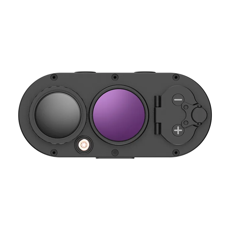
Ura-Z Series Dual-Light Fusion Handheld Thermal Observer
Deployment Classification: Fully Integrated Multi-Spectral Field Observation Device
The Ura-Z Series is a dual-light fusion handheld thermal observer built for outdoor search, site patrol, visibility enhancement, and field documentation workflows. Housed in an IP66 weather-sealed enclosure weighing 1.0 kg or less, it pairs a 640×512 uncooled VOx microbolometer array (12 μm pixel pitch) with an integrated low-light visible optical sensor. Featuring a 35 mm manual-focus lens delivering a 12.6° × 10.1° field of view, the Ura-Z Series provides long-range target acquisition across demanding industrial inspection, perimeter security, and rescue missions.
Comprehensive Technical Specifications
| Parameter | Preserved Manufacturer Specification |
|---|---|
| Thermal Resolution | 640 × 512 pixels |
| Pixel Pitch | 12 μm |
| Optical Lens Configuration | 35 mm manual focus objective lens |
| Field of View (FOV) | 12.6° × 10.1° |
| Observation Modes | Thermal mode, low-light visible mode, and dual-light fusion mode |
| Operating Temperature | -40°C to +50°C |
| Ingress Protection Rating | IP66 certified |
| Physical Dimensions | ≤ 153 × 150 × 68 mm |
| System Mass | ≤ 1.0 kg |
| Primary Applications | Outdoor search, industrial site patrol, safety and rescue, perimeter monitoring |
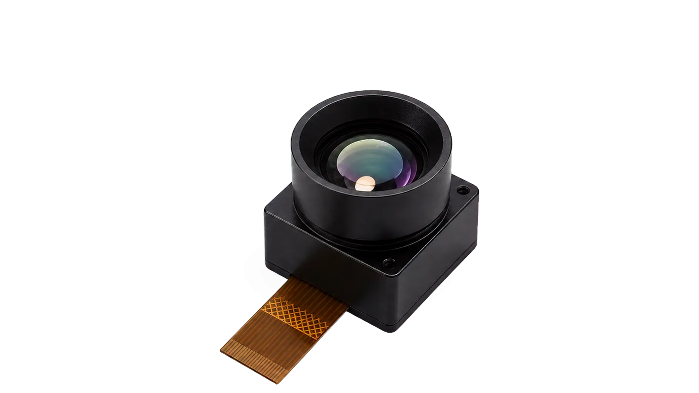
TC160-NF 160×120 Uncooled LWIR Thermal Imaging Module
Deployment Classification: Embedded OEM Thermal Core & Sensor Engine
The TC160-NF is an ultra-compact uncooled LWIR thermal module engineered for embedded hardware teams building smart sensors, HVAC diagnostic tools, low-power IoT devices, and OEM imaging sub-assemblies. Operating across the 8 to 14 μm spectral band, this bare board module outputs factory-calibrated radiometric thermal data over a high-speed SPI host interface while sipping just 76 to 78 mW on a 3.3 V DC rail. Equipped with a fixed-focus optical assembly (56° / 45° / 34° Diagonal / Horizontal / Vertical FOV), the TC160-NF provides a fast track from benchtop prototyping to high-volume production.
Comprehensive Technical Specifications
| Parameter | Preserved Manufacturer Specification |
|---|---|
| Product Model & SKU | TC160-NF (SKU: MI1602M5S) |
| Thermal Resolution | 160 × 120 pixels (19,200 total active pixels) |
| Detector Pitch | 35 μm (reference) |
| Spectral Range | 8 to 14 μm (LWIR band) |
| Max Frame Rate | Up to 25 FPS |
| Optical Field of View | 56° / 45° / 34° (Diagonal / Horizontal / Vertical) |
| Host Interface & Pinout | SPI interface; 10-pin FPC connector (0.5 mm pitch reference) |
| Supply Voltage & Power | 3.3 V DC; Low-power operation (~76 to 78 mW reference) |
| Operating Temperature Range | -20°C to +85°C (Reference) |
| Calibration Status | Factory-calibrated thermal radiometric output |
| Evaluation Ecosystem | USB evaluation path available through dedicated eval-board planning |
Direct Engineering Comparison: Turnkey Field Unit vs. Embedded Sensor Core
| Architectural Attribute | Ura-Z Series Dual-Light Observer | TC160-NF OEM LWIR Core Module |
|---|---|---|
| System Type | Handheld Field Observation System | Bare Embedded Sub-Assembly / Core |
| Thermal Array Dimension | 640 × 512 (327,680 pixels) | 160 × 120 (19,200 pixels) |
| Sensor Pitch Scaling | 12 μm high-density pitch | 35 μm (reference) robust pitch |
| Optical Focal Group | 35 mm manual-focus lens (12.6°×10.1°) | Fixed-focus narrow-angle lens (45° H-FOV) |
| Electrical Power Ingest | Integrated battery management & charging | 3.3 V DC input; 76 – 78 mW draw |
| Data Output Protocol | Internal display viewfinder & internal storage | Direct SPI streaming (10-pin FPC) |
| Environmental Enclosure | Fully sealed IP66 chassis (≤ 1 kg) | Unsealed bare PCBA (Host sealing required) |
6. Systems Engineering Integration, Thermal Drift, and RFQ Sourcing
Integrating a thermal module into custom hardware brings a whole set of electrical, mechanical, and thermal challenges you won’t encounter with regular visible cameras.
Electrical Noise Isolation and PCB Layout
Microbolometer ROICs read microvolt-level signal variations across the suspended pixel bridges. This makes uncooled LWIR cores exceptionally sensitive to switching power supply noise and high-speed digital crosstalk. To prevent image artifacts:
- ⚙️ Clean Power Rails: Feed the core’s 3.3 V, 1.8 V, or analog bias lines using dedicated ultra-low-noise Low-Dropout Regulators (LDOs) with a Power Supply Rejection Ratio (PSRR) >70 dB at 10 kHz. Keep voltage ripple strictly below 10 to 15 mV peak-to-peak, or you will see distinct vertical banding crawl across your thermal frames.
- ⚙️ Trace Impedance Control: Match high-speed trace impedances (50 Ω single-ended for high-frequency SPI lines, 100 Ω differential for MIPI CSI-2 pairs) between your host processor and the module connector. Always maintain a solid, unbroken ground reference plane directly under digital data pairs to prevent EMI from radiating into the sensitive bolometer frontend.
Thermal Isolation and Mechanical Packaging
Here’s a critical reality: a microbolometer measures incoming infrared radiation while sitting inside an enclosure that is itself emitting infrared radiation. Uneven thermal gradients across your camera housing will distort the sensor baseline, causing drift and inaccurate radiometric readings:
- 📌 Isolate High-Power Silicon: Keep heat-generating parts (application processors, 4G/5G modems, motor drivers, and PMICs) physically separated from the thermal core. Use copper heat pipes, thermal gap pads, or aluminum heat shields to channel heat toward the outer chassis and away from the optical barrel.
- 📌 Infrared Protective Windows: If you are sealing an OEM module inside an IP67 enclosure, standard glass, polycarbonate, or acrylic windows will completely block LWIR light. You must spec optical windows made from monocrystalline Germanium, Zinc Selenide (ZnSe), or Zinc Sulfide (ZnS). Specify a broadband anti-reflective (BBAR) coating tuned for 8 to 14 μm transmission, and add a Diamond-Like Carbon (DLC) exterior coating if the unit will face rain, sand, or harsh chemical washdowns.
Procurement Strategy and RFQ Checklist
When sending out a Request for Quotation (RFQ) for thermal hardware, giving the vendor a precise, complete engineering spec prevents redesign cycles and back-and-forth delays. Make sure your RFQ package covers:
- ⚙️ Target Standoff & FOV Requirements: Define target distance, physical target dimensions (person, vehicle, small PCB component), and required optical FOV (e.g., wide 45° horizontal FOV vs. narrow 12.6° FOV).
- ⚙️ Radiometric Accuracy & Temperature Envelope: State whether you need qualitative imaging (contrast only) or fully calibrated radiometric temperature output across specific ranges (e.g., -20°C to +150°C or high-temperature ranges up to +550°C).
- ⚙️ Host Bus Protocol & Electrical Envelope: Lock down hardware interface requirements (SPI, USB, MIPI CSI-2, connector pin pitch), available DC supply voltages, peak power limits, and physical enclosure dimensions.
- ⚙️ Environmental & Export Compliance: Detail ingress protection ratings (IP66, IP67), operating temperature limits (-40°C to +50°C), NDAA compliance requirements, and export classifications (EAR99 vs. Dual-Use ECCN 6A003 controls).
- ⚙️ Commercial Terms & Evaluation Units: Define prototype build quantities, expected annual volume ramps, warranty coverage, eval kit availability, and the manufacturer’s standard refund policy for technical hardware evaluations.
7. Frequently Asked Questions (Technical Deep-Dive)
Why do low-cost thermal cameras often fail in demanding industrial or field environments?
What is the practical difference between a standalone thermal camera and an OEM thermal core module?
How do resolution and lens focal length balance when selecting a thermal camera for field observation versus close-up inspection?
How does dual-light sensor fusion resolve optical parallax across varying target distances?
📚 References & Further Reading
- Edge AI Acceleration: Learn more about high-performance edge neural processors at Hailo AI.
- Emerging Electro-Optics Research: Discover breakthrough sensor and photonics analysis via the MIT Technology Review.
- OEM High-Resolution Design: Explore our comprehensive high-resolution thermal imaging camera OEM selection guide.
- Outdoor & Perimeter Imaging: Review deployment strategies for uncooled LWIR thermal modules for outdoor security and monitoring.
- Procurement & Commercial Policies: Review technical hardware procurement and return frameworks via the corporate refund policy.