Sierra Imaging & Thermal Vision: OEM Core Selection and Integration Guide
Sierra Imaging & Thermal Vision: OEM Core Selection and Integration Guide
Thermal imaging technology has completely moved past the days when it was locked inside classified defense labs or high-end aerospace payloads. Today, it serves as a frontline sensing modality across industrial automation, mobile robotics, condition monitoring, predictive maintenance, and embedded edge vision. Engineering teams hunting down thermal modules—often digging through technical catalogs and trade specs under search queries like sierra imaging and industrial thermal vision—quickly run into a brutal mix of analog physics, high-speed digital buses, precision optics, and tricky radiometric math. Specifying an uncooled long-wave infrared (LWIR) sensor requires an end-to-end grasp of microbolometer semiconductor physics, raw digital signal transport mechanics, optical engineering principles, and host-side radiometric firmware pipelines.
Here’s the deal: getting an uncooled thermal core into a commercial product demands a no-compromise balance across your SWaP-C budget (Size, Weight, Power, and Cost). Whether you are packing an infrared engine into a ruggedized handheld diagnostic gun, a factory-floor inspection rig, or an aerial inspection drone, you have to weigh detector resolution, thermal sensitivity, lens athermalization, bus bandwidth, and host processor loads. This architectural guide cuts through the marketing noise to give OEM systems architects, embedded hardware engineers, and technical procurement teams a battle-tested engineering blueprint for evaluating, selecting, and shipping uncooled LWIR thermal imaging modules.
Table of Contents
- 👉 1. Infrared Physics & Microbolometer Fundamentals
- 👉 2. Embedded Electrical Architectures & Signal Processing Pipelines
- 👉 3. Optical Engineering: Lens Geometry & Environmental Athermalization
- 👉 4. Industrial LWIR Core Technical Matrix & Product Analysis
- 👉 5. Host Firmware, Radiometric Calibration, and Edge AI Integration
- 👉 6. OEM Procurement Framework & Integration Verification Protocol
- 👉 7. Comprehensive Technical FAQ
1. Infrared Physics & Microbolometer Fundamentals
To successfully integrate thermal imaging cores, engineers must first analyze how uncooled microbolometers detect and transduce radiative thermal flux into usable digital data streams. Visible-spectrum CMOS image sensors rely entirely on reflected ambient photons in the narrow 0.4 µm to 0.7 µm spectrum. Thermal sensors do not care about illumination. Instead, they capture raw electromagnetic energy emitted directly by matter as a direct consequence of its thermodynamic temperature.
1.1 LWIR (8–14 µm) Transmission Dynamics & Thermal Flux
The infrared spectrum is sliced into distinct functional bands: Short-Wave Infrared (SWIR, 1–3 µm), Mid-Wave Infrared (MWIR, 3–5 µm), and Long-Wave Infrared (LWIR, 8–14 µm). In the uncooled industrial space, LWIR is the undisputed workhorse. Plain and simple: terrestrial objects operating between -40°C and +100°C (-40°F to +212°F) hit their peak spectral radiance squarely within this 8–14 µm corridor, governed by Planck’s Law of Blackbody Radiation and Wien’s Displacement Law.
When you run the math on Planck’s distribution for an ambient room-temperature object (~300 Kelvin), the peak emission wavelength sits at approximately 9.7 µm. Just as critical, Earth’s atmospheric chemistry produces a massive absorption notch between 5 µm and 8 µm caused by ambient water vapor and CO2. That makes the 8–14 µm band an open optical highway, allowing non-cryogenic sensors to pull crisp thermal signatures over long operational distances without getting wiped out by atmospheric attenuation.
The total radiant flux hitting your focal-plane array (FPA) depends on target emissivity, atmospheric loss, optical transmission efficiency, and the numerical aperture (f-number) of the objective lens assembly. The total thermal irradiance arriving at each microbolometer pixel is calculated as:
Irradiance (E) = [ τatm × τopt × ε × σ × T4 ] / [ 4 × (F/#)2 ]
Here, τatm is atmospheric transmission efficiency, τopt is the optical transmission coefficient of your infrared lens stack, ε represents the surface emissivity of the target (ranging from 0.05 for mirror-polished bare metal up to 0.98 for matte black anodized aluminum or human skin), σ is the Stefan-Boltzmann constant (5.670374 × 10⁻⁸ W·m-2·K-4), T is thermodynamic temperature in Kelvin, and F/# represents optical aperture speed. Neglect any of these variables in your optical path calculation, and your temperature readings will drift off target. For hands-on field calibration tutorials, check out our repository of Thermal Imaging Guides.
1.2 VOx vs. a-Si Focal Plane Arrays and Pixel Pitch Evolution
Uncooled thermal cores use a Focal Plane Array (FPA) populated by thousands of microbolometer pixels. Each pixel is an infrared-absorbing membrane suspended on micro-machined isolation bridges above an underlying silicon Readout Integrated Circuit (ROIC). Incident infrared photons strike the membrane, heat it up, and shift its bulk electrical resistance. The ROIC queries this resistance change by pulsing a precise bias voltage and integrating the output current.
In modern production, you will encounter two primary thermoresistive materials:
- ✅ Vanadium Oxide (VOx): Vanadium Oxide is the industry standard for high-performance thermal sensing. VOx delivers a high Temperature Coefficient of Resistance (TCR) typically between -2% and -3% per Kelvin, paired with low 1/f flicker noise. VOx arrays provide high thermal sensitivity, clean signal-to-noise ratios (SNR), and rock-solid stability during broad ambient thermal swings.
- ⚙️ Amorphous Silicon (a-Si): Amorphous Silicon FPAs can be manufactured on standard CMOS semiconductor lines, which keeps raw wafer processing costs down. The downside? a-Si materials carry higher intrinsic 1/f noise floors and lower thermal isolation efficiency compared to VOx, resulting in higher baseline Noise Equivalent Temperature Difference (NETD) numbers.
Over the last decade, pixel pitch has shrunk dramatically. Legacy thermal engines were built around 35 µm or 25 µm nodes. Today’s production lines center on 17 µm and 12 µm wafer processes. Shrinking the pixel pitch reduces the physical diagonal of the silicon die for any given resolution. A 12 µm 640×512 array takes up a fraction of the silicon real estate of an older 25 µm sensor. That means you can use shorter focal length lenses with significantly smaller outer element diameters while preserving your spatial resolution. For the mechanical engineer, that translates directly into massive savings in total system weight, barrel length, and optics cost.
1.3 NETD, Thermal Time Constants, and Responsivity Metrics
When you are evaluating vendor datasheets, focus on these three core detector specifications:
Noise Equivalent Temperature Difference (NETD): Expressed in millikelvins (mK), NETD represents the temperature delta at the target object that produces a signal equal to the internal noise floor of the core (SNR = 1). Lower is always better. Professional-grade uncooled modules spec NETD ratings of <40 mK or <50 mK at 25°C using an F/1.0 lens. A sensor rated at 40 mK easily pulls out fine thermal gradients—like hidden wall insulation gaps, internal fluid line leaks, or subtle PCB traces under light load—that get swallowed by static on a budget 100 mK sensor.
Thermal Time Constant (τ): This measures how quickly a suspended pixel membrane sheds its thermal energy and returns to equilibrium (specifically reaching 63.2% of its steady-state response). Industrial microbolometers operate with thermal time constants between 8 ms and 14 ms. If you run a high-frame-rate core (50 Hz or 60 Hz) on a high-speed pan-tilt unit or an agile drone without a sufficiently low time constant, quick panning will create noticeable thermal smearing and trailing artifacts across the frame.
Detector Responsivity (Rv): Responsivity measures the electrical output voltage swing per unit of incident radiant power, expressed in Volts per Watt (V/W). Pushing responsivity as high as possible while suppressing ROIC amplifier noise is critical for preserving contrast when tracking targets in low-delta scenes.
2. Embedded Electrical Architectures & Signal Processing Pipelines
Integrating an uncooled thermal core into an embedded board design requires pairing the module’s electrical bandwidth and power profile with the processing muscle of your host hardware, whether that is a low-power microcontroller or an edge computing multicore application processor.
2.1 Low-Power Bus Transport: SPI and I2C Implementation
For low-resolution thermal cores (such as 160×120 or 80×60 formats) destined for battery-powered diagnostic tools, smart thermostats, or remote IoT nodes, a Serial Peripheral Interface (SPI) is an efficient bus choice. SPI gives you a simple, synchronous serial pipeline that can be fed straight into the Direct Memory Access (DMA) engine of low-cost microcontrollers like an STM32, ESP32, or NXP i.MX RT crossover processor.
Let’s run the raw bandwidth numbers for a 160×120 pixel resolution module pushing 16-bit radiometric frame data at a 25 Hz update rate:
Bandwidth = 160 pixels × 120 pixels × 16 bits/pixel × 25 frames/sec = 7,680,000 bits/sec ≈ 7.68 Mbps
An SPI bus clocked between 15 MHz and 25 MHz handles this data throughput with comfortable headroom. This lets your embedded processor push raw thermal frames into memory buffers using hardware DMA channels without bogging down the main CPU execution loop. An auxiliary I2C or standard UART line runs alongside the SPI bus to handle configuration commands, register queries, shutter triggers, and integration mode adjustments.
2.2 High-Throughput Digital Video: DVP, BT.656, LVCMOS, and MIPI
Step up to a 640×512 array running at 50 Hz, and the data volume jumps significantly. A 16-bit uncompressed digital radiometric stream at 640×512 @ 50 Hz demands serious bus bandwidth:
Bandwidth = 640 × 512 × 16 bits × 50 frames/sec = 262,144,000 bits/sec ≈ 262.14 Mbps
Standard SPI buses cannot handle that throughput. You must move to parallel or high-speed differential serialization options:
- ⚙️ Digital Video Port (DVP) / Parallel LVCMOS: Carries 14-bit or 16-bit parallel data lines matched with Pixel Clock (PIXCLK), Horizontal Sync (HSYNC), and Vertical Sync (VSYNC). This architecture interfaces directly with hardware capture peripherals on FPGAs and application processors like the Rockchip RK3588 or NXP i.MX8 family.
- ⚙️ ITU-R BT.656: Embeds timing and sync codes directly into an 8-bit parallel stream, freeing up board space by dropping external sync lines when you only need a standard video feed without full 16-bit radiometric data.
- ⚙️ MIPI-CSI2: Modern industrial cores increasingly feature serialized differential MIPI-CSI2 lanes. This minimizes PCB track count, controls high-frequency electromagnetic interference (EMI), and feeds thermal data straight into native SoC hardware ISP pipelines.
- ⚙️ Analog Composite (PAL / NTSC): High-end modules often maintain an analog DAC output. This lets you drive legacy cockpit monitors, field displays, or analog drone transmitters with zero host software overhead.
To dive deeper into PCB routing, signal integrity, and carrier board design for high-throughput video cores, explore our technical deep dives on the CamCuda Engineering Blog.
2.3 Power Delivery, Noise Filtering, and Multi-Rail Topologies
Microbolometer ROIC stages deal with microvolt-level analog signals coming off the pixel membranes. Because of that sensitivity, thermal cores are vulnerable to power rail noise, switching ripple, and ground bounce.
To preserve NETD performance and keep horizontal rolling bands or fixed-pattern noise from degrading your image, keep these power delivery rules in mind during layout:
- ⚙️ Dedicated Linear LDOs: Never power your sensor’s analog inputs directly off switching buck regulators. Use dedicated ultra-low-noise, high Power Supply Rejection Ratio (PSRR > 80 dB at 100 kHz) Linear Low-Dropout regulators placed close to the module header pins.
- ⚙️ Ferrite Beads & Multistage Decoupling: Use high-impedance ferrite beads to isolate analog supply planes from noisy digital logic planes. Place a combination of 0.1 µF and 10 µF low-ESR ceramic decoupling capacitors right against the core’s input pins to ground high-frequency noise generated by the host SoC.
- ⚙️ Strict Multi-Rail Sequencing: Modules using multiple voltage rails (e.g., 1.8V for internal logic, 3.3V for digital I/O, 5V for analog bias) require strict power sequencing. Ramping rails out of order can trigger internal CMOS latch-up conditions that permanently damage the readout circuitry.
3. Optical Engineering: Lens Geometry & Environmental Athermalization
Designing optics for thermal imaging is entirely different from building visible-spectrum camera lenses. Standard optical glasses like BK7 or fused silica act like solid walls to 8–14 µm infrared light. LWIR optical assemblies rely on specialized infrared-transmissive materials, advanced anti-reflective coatings, and passive athermalization mechanics.
3.1 Optical Materials: Germanium vs. Chalcogenide Glass
Production LWIR lenses are built around two primary optical substrates:
Monocrystalline Germanium (Ge): Germanium remains the classic baseline for thermal optics. Its refractive index is exceptionally high (n ≈ 4.003 at 10 µm), allowing lens designers to build compact, fast, low-aberration assemblies with very few optical elements. However, Germanium carries a notable thermal drawback: a high thermo-optic coefficient (dn/dT ≈ 3.96 × 10⁻⁴ /°C) and an issue called thermal runaway. Cross 70°C, and Germanium experiences elevated free-carrier absorption, becoming opaque and blocking thermal transmission.
Chalcogenide Glass (e.g., Ge28Sb12Se60 / GASIR): Chalcogenide glass is an amorphous infrared material that can be precision-molded into complex aspheric and diffractive profiles at scale. Chalcogenide features a much lower dn/dT than Germanium, maintains steady transmission across -40°C to +85°C, and lowers optical bill-of-materials costs during high-volume manufacturing runs.
Both materials require high-efficiency Anti-Reflective (AR) or Diamond-Like Carbon (DLC) exterior coatings. Uncoated Germanium reflects roughly 36% of incident infrared energy per optical surface due to Fresnel reflection losses.
3.2 Passive Athermalization Across -40°C to +80°C
Industrial, aerospace, and outdoor surveillance modules must maintain sharp focus across extreme temperature swings (-40°C to +80°C). When temperatures shift across an uncompensated lens, three factors occur at the same time:
- ⚙️ Refractive Index Shift: The refractive index of the lens elements drifts significantly due to the material’s dn/dT coefficient.
- ⚙️ Curvature Expansion: Lens radii of curvature and element thicknesses expand or contract mechanically.
- ⚙️ Housing Expansion: The mechanical lens barrel (typically aluminum) expands or contracts, altering the back-focal distance between the optical rear vertex and the microbolometer FPA plane.
Without optical compensation, the focal plane drifts rapidly away from the sensor surface, destroying system Modulation Transfer Function (MTF) and turning crisp thermal scenes into an unusable blur. Motorized active focus assemblies can compensate for this drift, but they add unwanted weight, mechanical complexity, battery draw, and extra points of failure.
Passive Opto-Mechanical Athermalization fixes this by pairing lens elements made from complementary optical materials with a multi-material mechanical barrel (combining high-expansion materials like Delrin or Aluminum with low-expansion structural sleeves like Invar). The mechanical expansion of the barrel offsets the optical focal shift across the full operating range, maintaining crisp focus without moving parts or firmware adjustments.
3.3 Instantaneous Field of View (iFOV) & DRI Calculations
To map target detection capabilities for your integrated system, optical engineers calculate Field of View (FOV) alongside Instantaneous Field of View (iFOV). The iFOV defines the angular footprint mapped onto a single microbolometer pixel:
iFOV (milliradians) = [ Pixel Pitch (µm) / Focal Length (mm) ]
Target acquisition ranges are quantified using Johnson’s Criteria, standardized across international defense and industrial surveillance protocols (STANAG):
- ⚙️ Detection: Spotting an anomaly requires at least 1.5 to 2.0 pixels across the critical dimension of the target. An operator or vision algorithm can confirm a thermal delta exists against the background.
- ⚙️ Recognition: Classifying the target type (e.g., telling a human from a quadruped animal, or a sedan from a delivery van) demands 6.0 to 8.0 pixels across the critical dimension.
- ⚙️ Identification: Discerning specific features (e.g., distinguishing between a civilian truck and a utility vehicle, or confirming handheld tools) requires 12.8 or more pixels across the target silhouette.
When long-range target acquisition demands an integrated system, explore our complete technical overview of the URA-Y Series 640×512 Handheld Thermal Observation Binoculars.
4. Industrial LWIR Core Technical Matrix & Product Analysis
Selecting the right core comes down to aligning system requirements with the physical, electrical, and optical properties of available hardware. Below is a side-by-side technical evaluation of two industrial LWIR cores: the ultra-compact, low-power TC160-NF and the high-definition Mini 640 (9.1 mm).
4.1 TC160-NF: Ultra-Low-Power 160×120 SPI Module
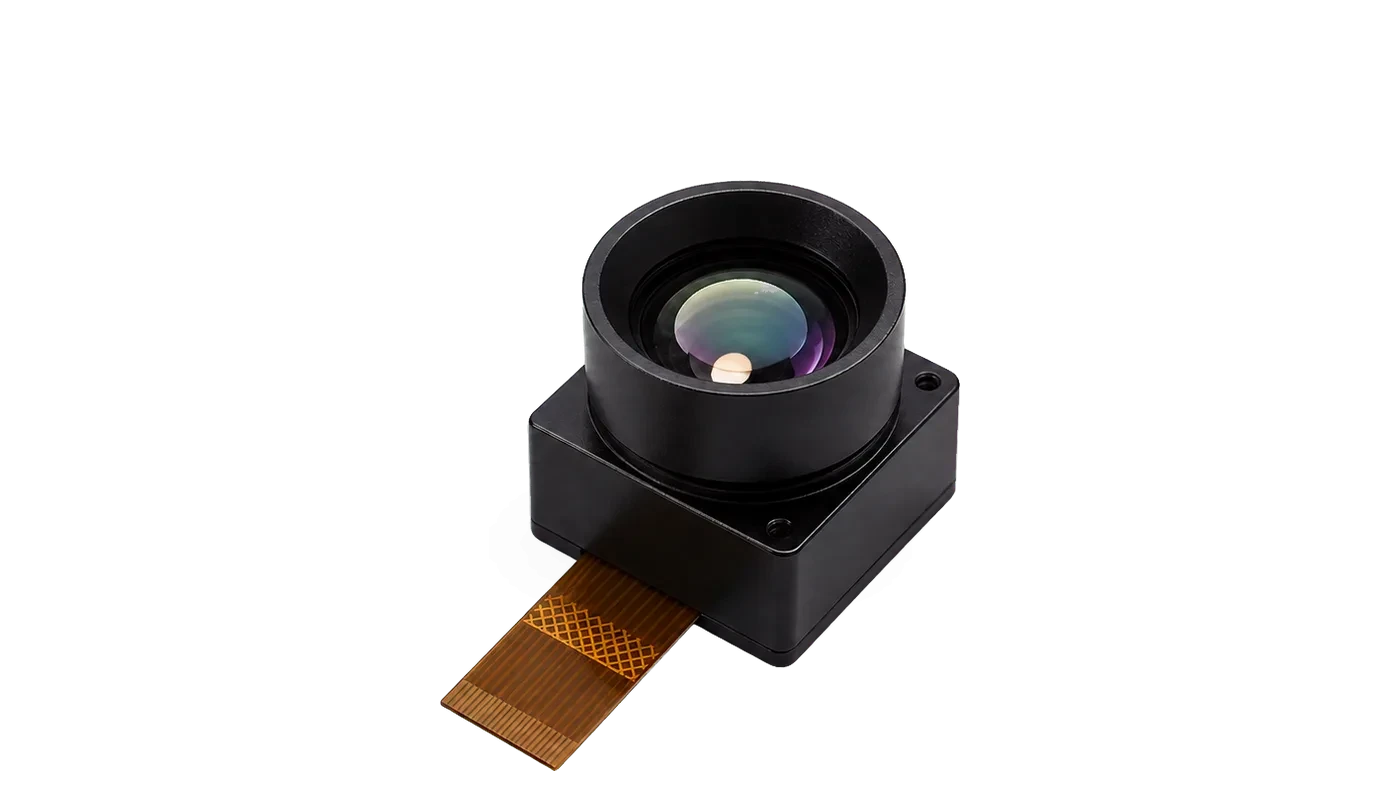
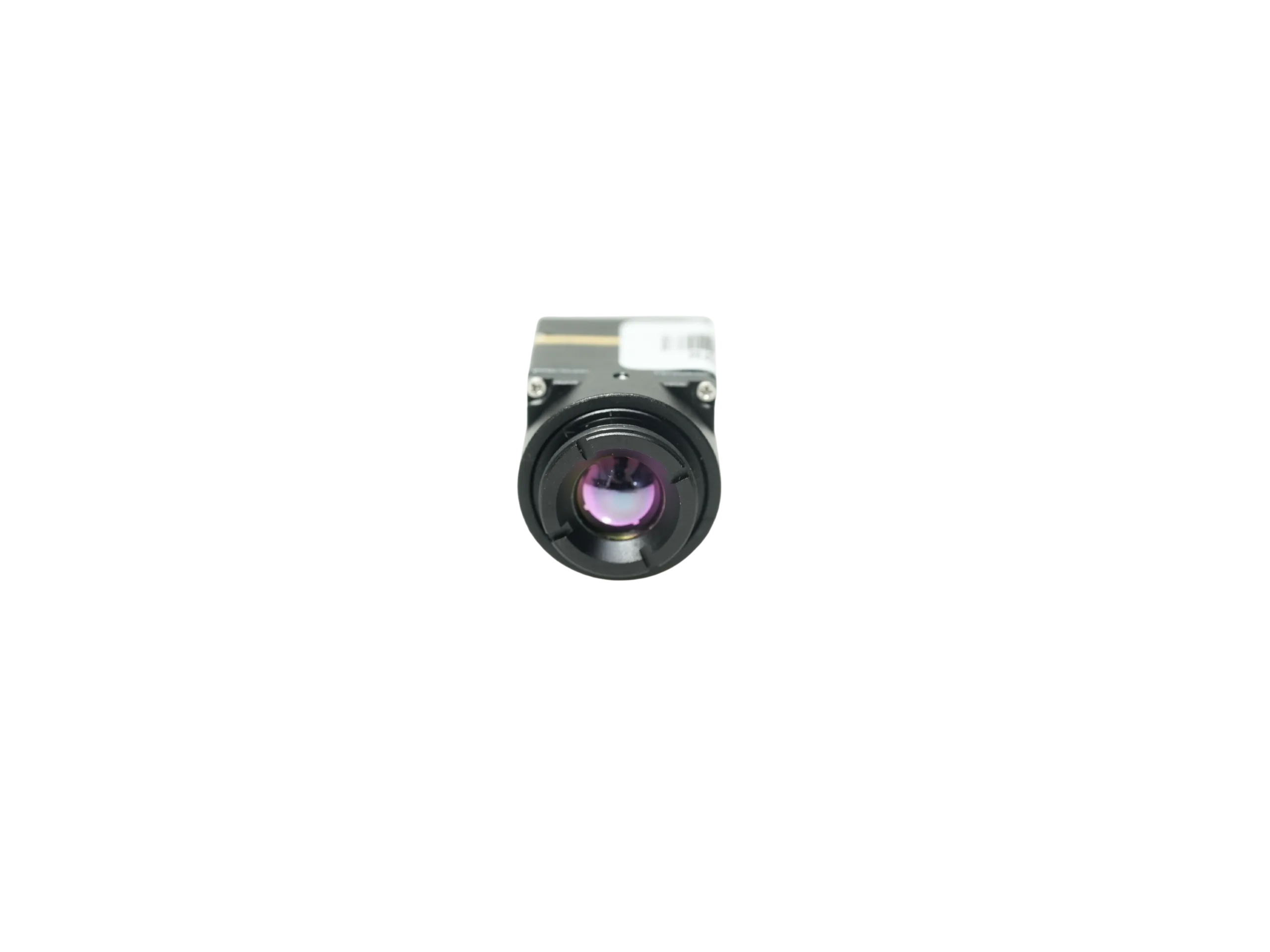
Figure 1: TC160-NF Compact 160×120 Uncooled LWIR Thermal Imaging Core
The TC160-NF is an ultra-compact uncooled LWIR core purpose-built for space-constrained, battery-powered embedded systems, smart home hardware, localized HVAC diagnostics, and compact industrial IoT nodes. Drawing just 76–78 mW on a 3.3 V single-rail supply, it ties directly into host microcontrollers via an embedded SPI interface.
Featuring a 160×120 resolution array (19,200 active pixels) operating across the 8–14 µm spectral band at up to 25 FPS, the TC160-NF delivers factory-calibrated radiometric frame data. Its integrated narrow-FOV optical stack ($56^\circ \text{ D} / 45^\circ \text{ H} / 34^\circ \text{ V}$) provides balanced spatial coverage for mid-range condition monitoring, connecting via a 10-pin 0.5 mm pitch Flexible Printed Circuit (FPC) interface.
Comprehensive TC160-NF Engineering Specifications
| Parameter Category | Engineering Specification Value |
|---|---|
| Product Model & SKU | Model: TC160-NF | SKU Reference: MI1602M5S |
| Detector Resolution | 160 × 120 pixels (19,200 active elements) |
| Pixel Pitch & Spectral Band | 35 µm reference pitch | 8–14 µm Long-Wave Infrared |
| Maximum Output Frame Rate | Up to 25 FPS (Smooth real-time temporal output) |
| Optical Configuration & FOV | Narrow-FOV fixed optics: 56° Diagonal / 45° Horizontal / 34° Vertical |
| Operating Voltage & Power | 3.3 V DC input | ~76 mW to 78 mW typical operating consumption |
| Host Data & Control Interface | SPI (Video stream/data) with 10-pin 0.5 mm pitch FPC path |
| Operating Temperature Envelope | -20°C to +85°C industrial operational rating |
| Calibration & Evaluation Path | Factory-calibrated radiometric output; USB evaluation kit available |
View Product Details & Pricing ➔
4.2 Mini 640 (9.1 mm): High-Definition 640×512 Embedded Vision Core
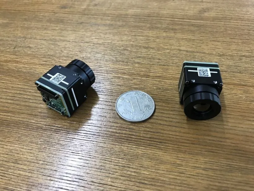
Figure 2: Mini 640 Core with Integrated 9.1 mm Athermalized Fixed-Focus Lens
The Mini 640 9.1 mm is a high-resolution uncooled LWIR core engineered for OEM integration into UAV gimbals, autonomous mobile robots (AMR), industrial machine vision, handheld thermography, and automated security turrets. It features an uncooled Vanadium Oxide (VOx) Wafer-Level Packaged (WLP) focal plane array running 640×512 resolution at a compact 12 µm pixel pitch.
Fitted with a 9.1 mm fixed-focus athermalized lens assembly, the Mini 640 covers an expansive field of view measuring 45.8° Horizontal × 37.3° Vertical. NETD sensitivity comes in at <50 mK at 25°C, F/1.0 (<40 mK optional), resolving minute thermal deltas in flat-gradient environments. Supporting 25 Hz or 50 Hz frame rates, the module provides flexible output modes: PAL/NTSC composite, parallel DVP, BT.656, and LVCMOS, alongside UART, I2C, and RS-232 serial control.
Comprehensive Mini 640 (9.1 mm) Engineering Specifications
| Parameter Category | Engineering Specification Value |
|---|---|
| Product Configuration | Mini 640 Core, 9.1 mm fixed-focus athermal optical assembly |
| Detector Technology | Uncooled VOx Focal Plane Array, Wafer-Level Packaging (WLP) |
| Array Format & Pixel Pitch | 640 × 512 pixels (327,680 total) | 12 µm pixel pitch |
| Spectral Range & Sensitivity | 8–14 µm LWIR | NETD <50 mK @ 25°C, F/1.0 (<40 mK optional) |
| Temporal Frame Rate | 25 Hz / 50 Hz options (Dependent on regional export/BOM configuration) |
| Optics & Calculated Sensor FOV | 9.1 mm athermal lens | Approx. 45.8° Horizontal × 37.3° Vertical FOV |
| Electrical Power Consumption | 1.8 V / 3.3 V / 5 V rails | Typical system consumption ~0.60 W |
| Video Output Formats | Digital: DVP / BT.656 / LVCMOS | Analog: PAL / NTSC composite |
| Command & Control Interfaces | UART / I2C / RS-232 serial interfaces (Board variant dependent) |
| Operating Environmental Envelope | -40°C to +80°C operational temperature rating |
View Product Details & Pricing ➔
4.3 Direct Parameter Comparison Table
The comparative matrix below matches core technical parameters side-by-side to assist embedded designers in selecting the appropriate core architecture for their product requirements:
| Engineering Metric | TC160-NF Module | Mini 640 (9.1 mm Configuration) |
|---|---|---|
| Native Array Resolution | 160 × 120 (19,200 pixels) | 640 × 512 (327,680 pixels) |
| Pixel Pitch | 35 µm reference | 12 µm VOx WLP |
| Spectral Range | 8–14 µm (LWIR) | 8–14 µm (LWIR) |
| Thermal Sensitivity (NETD) | Standard response (Factory calibrated) | <50 mK @ 25°C, F/1.0 (<40 mK optional) |
| Frame Rate Capabilities | Up to 25 FPS | 25 Hz / 50 Hz |
| Optical System & FOV | Narrow-FOV (56° D / 45° H / 34° V) | 9.1 mm Athermal (45.8° H × 37.3° V) |
| Digital Host Video Interface | SPI (Synchronous Serial) | DVP / BT.656 / LVCMOS / Analog PAL/NTSC |
| Command Interface | I2C / UART via FPC | UART / I2C / RS-232 |
| Nominal Power Consumption | ~76 mW to 78 mW (3.3 V single rail) | ~0.60 W (1.8 V / 3.3 V / 5 V rails) |
| Physical Connection Format | 10-pin FPC (0.5 mm pitch) | Multi-pin high-density board-to-board |
| Operational Temperature | -20°C to +85°C | -40°C to +80°C |
| Primary Target Applications | Smart appliances, HVAC, compact IoT sensing | UAV gimbals, robotics, handheld vision, security |
5. Host Firmware, Radiometric Calibration, and Edge AI Integration
Pulling raw analog-to-digital converter (ADC) counts out of the core is only stage one. Microbolometer FPAs require firmware-side DSP processing on the host processor to strip out spatial fixed-pattern noise, apply radiometric math, and shape the data stream for downstream edge AI inference.
5.1 Non-Uniformity Correction (NUC) & Bad Pixel Replacement
Due to semiconductor manufacturing tolerances, every individual microbolometer pixel on the array has a slightly different responsivity slope (gain) and baseline dark current (offset). Left uncorrected, this creates Fixed-Pattern Noise (FPN)—a static mesh pattern overlaid on your live image.
To eliminate FPN, firmware pipelines execute a two-point Non-Uniformity Correction (NUC):
Scorrected(x, y) = Gain(x, y) × [ Sraw(x, y) – Offset(x, y) ]
The per-pixel gain matrix is baked into onboard flash during factory blackbody calibration. The offset matrix, however, drifts continuously as the sensor’s housing changes temperature during operation. The core recalibrates this offset by firing an internal mechanical shutter—or running a shutterless algorithm—to present the detector with a uniform thermal reference for a few frames.
Along with NUC, Bad Pixel Replacement (BPR) routines spot dead, saturated, or erratic pixels that fall outside normal tolerances. The host firmware replaces these defective pixels in real time using 3×3 or 5×5 median filters calculated from surrounding active pixels.
5.2 Radiometric Calibration LUTs and Thermal Scaling
Radiometric cores output calibrated 14-bit or 16-bit counts that correspond directly to object surface temperatures. Converting raw ADC values into engineering units requires modeling Planck’s radiative transfer curve alongside atmospheric and reflected temperature offsets.
In the shop, we keep embedded routines lean. The following C function demonstrates a fixed-point linear conversion used in embedded firmware to turn raw 14-bit pixel data into absolute Kelvin temperatures:
/*
 * Embedded C99 Linear Radiometric Transfer Function
 * Converts raw 14-bit digital counts into centikelvin (cK: 30000 cK = 300.00 K = 26.85 °C)
 */
#include <stdint.h>

int32_t CalculatePixelTemperature(uint16_t raw_pixel_adu, float target_emissivity, float reflected_temp_k) {
    if (target_emissivity <= 0.01f) {
        target_emissivity = 0.01f; // Prevent division by zero
    }

    // Step 1: Compensate for object surface emissivity
    float corrected_flux = (float)raw_pixel_adu / target_emissivity;

    // Step 2: Linear transfer mapping (calibrated slope m = 0.04, offset b = 273.15 K)
    // Translates 14-bit ADU count into centikelvin units
    float absolute_kelvin = (corrected_flux * 0.04f) + 273.15f;
    int32_t temp_centikelvin = (int32_t)(absolute_kelvin * 100.0f);

    return temp_centikelvin;
}
5.3 Edge AI Integration for Inference Pipelines
Streaming uncooled LWIR data into edge AI platforms (like NVIDIA Jetson, NXP i.MX8M Plus, or Rockchip RK3588 NPUs) unlocks automated human/vehicle classification, perimeter boundary alerts, and thermal fault detection that work completely independent of ambient lighting.
Edge AI inference pipelines require dedicated pre-processing steps:
- ⚙️ High Dynamic Range (HDR) Tone Mapping: Microbolometers output 14-bit linear dynamic range (0 to 16,383 levels), but standard Convolutional Neural Networks (CNNs) like YOLOv8 or SSD MobileNet expect 8-bit inputs (0 to 255 levels). Simple linear downscaling flattens low-contrast thermal edges. To solve this, host pre-processing pipelines use Contrast Limited Adaptive Histogram Equalization (CLAHE) or bilateral filtering to compress the dynamic range while preserving critical edges.
- ⚙️ Thermal-Specific AI Training: Models trained on standard ImageNet or COCO RGB datasets perform poorly on thermal inputs because thermal video lacks color channels and visible surface textures. Edge AI networks must be fine-tuned on annotated thermal datasets that account for thermal bloom, hot-spot reflections, and diurnal environmental inversions.
6. OEM Procurement Framework & Integration Verification Protocol
When drafting your formal Request for Quotation (RFQ) for thermal imaging modules, follow this verification checklist to avoid costly board revisions and supply chain delays:
OEM Specification & Procurement Checklist
- ✅ Mechanical Envelope & Enclosure Needs: Lock down maximum dimensions, mass limits, optical focal length, field-of-view requirements, lens athermalization ranges (-40°C to +80°C), and environmental sealing requirements (bare board module vs. IP67 front element).
- ✅ Host Bus Routing: Select your primary data interface (SPI for low-power microcontrollers vs. parallel DVP / BT.656 / MIPI for high-definition streaming). Verify power rail sequencing, current headroom, and connector footprints (FPC ribbon vs. board-to-board mezzanine headers).
- ✅ Radiometry vs. Visual Output: Decide early if you need per-pixel absolute temperature calculation (radiometric) or qualitative visual output (image-only with on-core AGC).
- ✅ Regulatory & Frame Rate Compliance: Frame rates above 9 Hz (like 25 Hz or 50 Hz) are dual-use commodities subject to international export controls (such as US EAR or EU Dual-Use rules). Confirm target markets and end-use paperwork early in development.
- ✅ Volume Pricing & Prototype Support: Account for sample costs, carrier board kits, SDK and documentation access, and volume tiers before signing production contracts.

7. Comprehensive Technical FAQ
How does embedded thermal sensor imaging differ from operating system disk imaging?
What host interface should be chosen for embedded thermal modules?
How do optical selection and athermal lenses affect thermal imaging accuracy?
What is the operational difference between radiometric and image-only (non-radiometric) thermal cores?
📚 References & Further Reading
- Industry Standard: Wikipedia – Infrared Physics & Transmission Dynamics
- Industry Standard: Wikipedia – Edge Computing Architectures
- Related Guide: CamCuda Thermal Imaging Technical Guides
- System Architecture: CamCuda Engineering Blog & Embedded Vision Resources
- Integrated Systems: URA-Y Series 640×512 Handheld Thermal Observation Binocular